

About the Cover:
Spotlights on Applications

Strategically Advancing Semiconducting Phthalocyanines as High-Performance Electrocatalysts for Electrochemical CO2 Reduction
Tengyi Liu *- ,
Xiaofan Hou - ,
Di Zhang - ,
Yutaro Hirai - ,
Kosuke Ishibashi - ,
Yasutaka Matsuo - ,
Shimpei Ono - ,
Hao Li *- , and
Hiroshi Yabu *

This publication is Open Access under the license indicated. Learn More
Phthalocyanines (Pcs) are promising organic molecular catalysts owing to their well-defined structure and metal–nitrogen sites. However, their application in energy conversion processes, such as electrochemical CO2 reduction (ECR), is severely hindered by intrinsically limited semiconducting conductivity. Conventional chemical intuitions suggest that effective catalytic performance can only be achieved through molecular-level dispersion of Pcs on carbon supports; nevertheless, such strategies are inherently difficult to scale in practical systems. To overcome these challenges, herein, we propose two complementary approaches that fundamentally enhance the performance of Pc-based electrocatalysts. First, crystallization engineering is employed to construct multilayer cobalt phthalocyanine (CoPc) assemblies that form crystallized architectures on conductive substrates. This design markedly improves charge transport, thereby enhancing ECR activity, while simultaneously offering a scalable and practical route for fabricating Pc crystal electrodes. Second, the incorporation of pyridinic nitrogen into the Pc macrocycle yields cobalt tetra-aza-phthalocyanine (CoTAP). This catalyst exhibits record-high current density, mass activity, and operational stability, which can be attributed to an optimized electronic structure and more favorable adsorption of reaction intermediates. Collectively, these strategies overcome the intrinsic semiconducting limitations of conventional Pcs and establish a scalable framework for advancing molecular electrocatalysts toward high-performance electrochemical CO2 reduction technologies.
Reviews
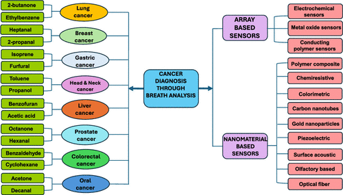
Advances in Volatile Organic Compounds-Based Biomarker Detection Using Nanomaterial-Integrated Sensor Platforms for Cancer Diagnosis
Swati Checker - ,
Aniruddh Bahadur Yadav *- ,
G. V. Sivnath Reddy - , and
Rahul Checker
Volatile organic compounds (VOCs) in exhaled breath have been reflected in many human diseases, including cancers. Cancerous cells produce several VOCs composed of hydrogen, oxygen, and carbon due to specific biological processes such as oxidative stress and inflammation. These VOCs are currently used as biomarkers for the early diagnosis of different cancers to improve the survival rate. Numerous electronic devices have been employed to classify these VOCs, for example, transistors, diodes, and other nanomaterial-based sensors. The need to develop diagnostic and detection methodologies for an increasing number of clinical challenges is escalating each year. In this review, we present a concise yet informative overview of the recent advancements in nanosensors and the use of VOCs for cancer diagnosis. VOCs found in exhaled breath have shown promising results as biomarkers for various cancer types. Advancement in colorimetric sensor array technology, functionalized gold nanoparticles, surface acoustic wave sensors, breath collection methods, and clinical phenotyping has significantly enhanced the accuracy of breath-based biomarkers. Nanomaterials are ideal for such sensor arrays due to ease of fabrication, chemical versatility, and compatibility with currently available sensing platforms. Following a general introduction and background of VOCs, we provide a brief description of VOC-related disease mechanisms. We then focus on volatile biomarkers identified in different types of cancer and the detection of VOC-related biomarkers using both selective and cross-reactive sensing approaches. These approaches utilize mechanical, chemical, and optical transducers incorporating the most relevant classes of nanomaterials. We conclude with a discussion on the potential integration of various nanomaterials into sensor arrays along with anticipated outcomes and current limitations.
Articles

Boron-Assisted Epitaxial Growth of Buffer-Layer-Free Graphene on the Si-Face of SiC without 30° Rotation
Rei Hobara *- ,
Ryota Akiyama - , and
Shuji Hasegawa
Graphene grown by thermal decomposition of SiC has attracted significant attention due to its scalability and direct synthesis on the wide-bandgap semiconductor substrate. Conventional epitaxial growth on the Si-face of 4H-SiC typically results in 30°-rotated (R30) graphene that is strongly coupled to the substrate via a buffer layer that is a deformed honeycomb lattice of carbon exhibiting a (6√3 × 6√3)R30° periodicity. Here, we report an epitaxial growth mode enabled by boron, resulting in graphene without 30°-rotation (R0) and without the formation of the buffer layer between graphene and SiC. This growth occurs at relatively low temperatures (∼1450 °C) despite the use of an Ar atmosphere. The number of layers of R0-aligned graphene varies depending on the growth temperature, but all layers exhibit no detectable rotational misalignment, as confirmed by reflection high-energy electron diffraction (RHEED) and transmission electron microscopy (TEM). TEM also reveals an enlarged interlayer spacing around 3.5 Å and non-Bernal, translationally random stacking indicative of weakened interlayer coupling. Electron energy loss spectroscopy (EELS) shows a high concentration of boron confined to the graphene/SiC interface and a smaller amount within the graphene layers. Raman spectroscopy confirms the absence of the buffer layer and indicates that substitutional boron, if present, accounts for only a small fraction of the total boron. These results demonstrate that boron-assisted growth fundamentally alters the interfacial chemistry and stacking sequence of epitaxial graphene on SiC, enabling R0-aligned, buffer-layer-free multilayer graphene.
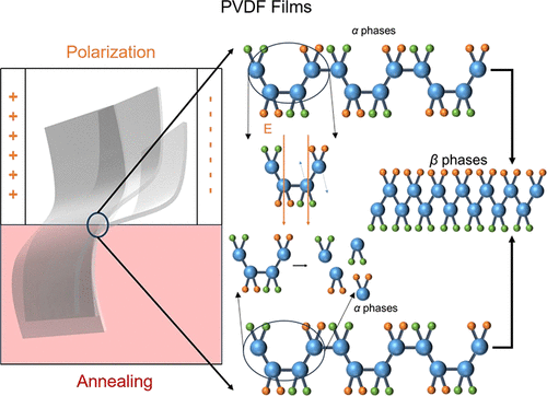
Dispensing Printing for Microelectronics and Vibration Performance of PVDF Films
Xuyuan Kou - ,
Lingke Zhu - ,
Baiqi Jing - ,
Yan Wang - ,
Nina Dai - ,
Fei Jing - ,
Gexia Yuan *- , and
Dengwei Hu *
Flexible piezoelectric films are increasingly vital for advanced electronic devices, where higher sensitivity and enhanced piezoelectric performance are in growing demand. Polyvinylidene fluoride (PVDF) is particularly notable for its strong piezoelectric effect, flexibility, chemical stability, and tunable piezoelectric properties, making it an excellent candidate for flexible electronics. Improving the piezoelectric performance of PVDF films thus remains a key challenge in device fabrication. In this work, PVDF films were prepared using a microelectronic printing method followed by a combined heat treatment and electrode polarization process. We systematically studied their ferroelectric and dielectric properties, energy harvesting performance, and deformation vibration behavior. Finite element simulations were also conducted to analyze the piezoelectric response, breakdown pathways at maximum voltage, and voltage output under mechanical loading. Results show that films printed with 24% solid content, dried at 40 °C, and subjected to coupled heat and polarization treatment exhibit increased β-phase content. This leads to a higher maximum breakdown voltage and enhanced residual polarization, along with an improved dielectric constant and reduced dielectric loss. These changes contribute to superior energy harvesting efficiency and larger vibration amplitude. The optimized films achieved an open-circuit voltage of 15.51 V and short-circuit current of 5.34 μA during energy harvesting tests. This study provides a practical and effective process optimization route for fabricating high-performance PVDF thin-film devices, demonstrating significant application potential in flexible electronics.

Smartphone-Assisted Detection of Homocysteine in Serum Using Boron–Nitrogen Co-doped MXene and MWCNTs
Indrani Nandi - ,
Rohini Kumari - ,
Riddhi Dubey - ,
Ankur Singh - , and
Pranjal Chandra *
Chronic illnesses such as cardiovascular disease (CVD) are currently among the biggest risks to human health. The accumulation of homocysteine (Hcy) can result in platelet disorders, vascular damage, smooth muscle swelling, and ultimately occlusive thrombus development, all of which raise the risk of CVD. Hence, the sensitive and selective detection of Hcy, a critical biomarker for cardiovascular disorders, is vital for early diagnosis and clinical monitoring. In this study, we created an electrochemical sensor for the detection of Hcy using an electrode modified with a nanohybrid comprising boron–nitrogen (B–N) codoped MXene (BNM) and multiwalled carbon nanotubes (MWCNTs). The codoping of B and N increases the dispersion of MXenes, greatly expanding the effective surface area and giving a large number of electroactive sites for MWCNTs, while MWCNTs enhance electrocatalysis and inhibit restacking. Thus, both materials in conjunction can result in superior electrochemical properties. Under optimized conditions, the developed sensor exhibited excellent efficiency for Hcy detection, with a wide linear range of 2.5–400 μM, which covers the normal as well as clinical range. It possesses a detection limit of 0.39 ± 0.02 μM and a response time of 2.6 ± 0.14 s. The sensor demonstrated high selectivity in the presence of common interfering species and excellent reproducibility and stability, making it suitable for practical applications. Furthermore, the smartphone application “HomoCysCheck” was developed to rapidly calculate Hcy concentrations and distinguish between safe and unsafe levels in real samples. This work provides a simple and rapid detection platform for Hcy, offering significant potential for use in point-of-care applications.

Trimodal Hybrid Nanogenerators Comprising Thermoelectric, Triboelectric, and Piezoelectric Effects in Stretchable, All-in-One Energy Harvesting Modules
Injamamul Arief *- ,
Sayan Chakraborty - ,
Beate Krause *- ,
Titash Mondal - ,
Petra Pötschke - ,
Sven Wiessner - , and
Amit Das
Hybrid nanogenerators are ubiquitous in today’s energy-intensive society and operate as self-powered systems that have wide-ranging applications in environmental monitoring, medical, and Internet-of-things-based devices. Triboelectric and piezoelectric devices operate on the principle of mechanical-to-electrical energy conversion, while thermoelectric devices are defined by their ability to convert thermal energy into scalable electrical outputs. In this work, we report a multimodal all-in-one nanogenerator based on a BaTiO3 (BTO)-decorated single-walled carbon nanotube (BTO@SWCNT) elastomer composite system, which harvests energy via triboelectric, piezoelectric, and thermoelectric effects. A liquid polyisoprene rubber matrix was employed as a matrix for the filler systems and subsequently modified using stencil printing to create a flexible device. The internal coupling of piezoelectric and triboelectric modes in a single composite layer yields significantly enhanced open-circuit voltages of 119 V (at 5 Hz), nearly twice the magnitude of that containing pristine SWCNT (65 V). The improvement is attributed to piezoelectric charge generation from the embedded BTO nanoparticles and enhanced interfacial polarization, which together boost charge density while avoiding excessive conductivity. The composite also exhibited an increased Seebeck coefficient of ∼77 μV K–1 and a power factor of 7.8 × 10⁻³ W m–1 K–2, as compared to that containing pristine SWCNTs (62 μV K–1 and 0.28 W m–1 K–2). Morphological studies reveal successful nanoscale integration of BTO on SWCNT surfaces, forming percolating networks at ultralow filler loadings (∼0.05 wt %). Mechanical tests confirm that the hybrid filler reinforces the rubber matrix without sacrificing flexibility. Our work highlights a promising materials strategy for self-powered systems by integrating high-dielectric piezoceramics with conductive nanostructures in a soft polymer, paving the way for versatile wearable energy harvesters.

Ionic-Based Electrochemical Gas Sensors for Low-Cost, High-Sensitivity SO2 Detection
Francisco Lagunas *- ,
Hacksung Kim - ,
Ella Myslo - ,
Nick Schimp - ,
Zachary D. Hood - , and
Jianlin Li
Sulfur dioxide (SO2) is a toxic gas associated with adverse health and environmental effects that necessitate reliable monitoring techniques. Here, we report the development of an all-solid-state electrochemical sensor utilizing a lithium borate (Li3BO3) solid electrolyte capable of subppm of SO2 detection. While subppm of SO2 sensing has been previously demonstrated in other solid-state electrolyte systems─such as stabilized zirconia, natrium super ionic conductors (NASICON) under mixed-potential conditions─here we establish Li3BO3 as an alternative solid electrolyte enabling equilibrium potentiometric sensing in an all-solid architecture. This sensor demonstrates a detection limit of at least 0.25 ppm, surpassing the human-olfactory threshold and meeting the rigorous requirements for industrial and personal monitoring applications. The sensing mechanism relies on the formation of Li2SO4 on the electrode surface, as evidenced by multimodal characterization techniques, including Raman spectroscopy, scanning electron microscopy (SEM), and scanning transmission electron microscopy (STEM). The strong linear correlation between the open-circuit potential (OCV) and the logarithm of SO2 concentration between 0.25 and 2 ppm indicates that the response is Nernstian in nature.
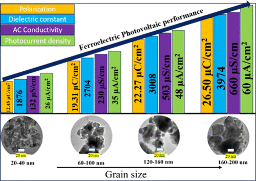
Optimizing the Ferroelectric Photovoltaic Performance of 0.9[KNbO3]–0.1[BaNi1/2Nb1/2O3−δ] Ceramics via Grain Size Engineering
Ankit Chahar - and
Balaji Birajdar *
This study elucidates the pivotal role of grain size engineering in enhancing the ferroelectric photovoltaic (FPV) performance of 0.9[KNbO3]–0.1[BaNi1/2Nb1/2O3−δ] [KBNNO] ceramics. A series of samples with grain sizes varying from 10 to 200 nm were synthesized via tailored sintering conditions. The grain growth significantly enhances ferroelectric polarization (from 12.45 to 26.50 μC/cm2) and increases the dielectric constant (from 1876 to ∼3974 at 1 Hz) while maintaining the band gap in the visible region of the solar spectrum. Concurrently, the reduction in the grain boundary density suppresses charge-carrier recombination and strengthens conductive pathways, as evidenced by the increase in the alternating-current conductivity (from 132 to 660 μS/cm). These improvements directly contribute to a superior photovoltaic performance, with the photocurrent density increasing from 26 to 60 μA/cm2, whereas the short-circuit current density increases from 5 to 9 μA/cm2. Further, the poling of KBNNO ceramics enhances the photoresponse of this material as the photocurrent density after the poling reached a maximum value of 101 μA/cm2 with a maximum short-circuit current density of 15.31 μA/cm2. Collectively, grain growth is a vital design parameter for optimizing the FPV performance and provides a comprehensive multiscale framework linking microstructural and functional properties in electroceramics.

Mechanically Induced Surface Metallization of Ultraflexible Liquid Metal/SEBS Fibers for On-Demand and Multifunctional Physiological Monitoring
Yidong Peng - ,
Ning Zhang *- ,
Haoran Liu - ,
Yuxi Zhang - ,
Tianxi Liu - ,
Yunpeng Huang *- ,
Ming Weng *- , and
Jihong Wang *
Fiber-based electronics are emerging as promising platforms for smart textiles, human-machine interfaces, and soft robotic systems, yet their practical deployment is hindered by limited conductivity and low structural robustness. Here, we report ultraflexible styrene-ethylene-butylene-styrene (SEBS) fibers homogeneously embedded with liquid-metal particles (LMPs) that undergo mechanically induced surface metallization, achieving an on-demand transition from insulating to conductive states for reliable motion sensing and high-fidelity electrophysiological monitoring. Micron-sized LMPs are homogeneously dispersed into an elastomer matrix to form a confined microstructure with strong antioxidation and leakage-free capabilities. Upon roller extrusion, the oxide shells of LMPs rupture, and eutectic gallium–indium extrudes and coalesces on the fiber surface, forming a stable and deformable metallized layer. This layer adheres strongly due to the high surface tension of liquid metal, imparting durable conductivity under repeated and large-scale deformation. These liquid metal fibers are further woven into permeable electronic textiles via a warp-weft manner, which simultaneously serve as strain sensors and epidermal bioelectrodes for stable motion sensing, and high-fidelity acquisition of surface electromyogram (sEMG), electrocardiogram (ECG), patterned visual evoked potentials (P-VEPs), and electrooculography (EOG) signals. This work establishes a scalable strategy to create on-demand, multifunctional fiber electronics for next-generation wearable bioelectronics.
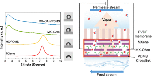
Hydrophobic-Modified, Stable MXene Membrane Joule Heater for Water Purification
Ki Hyun Lee - ,
Hyeonhoo Lee - ,
Hwansoo Shin - ,
Dong Jun Kang - ,
Yeongbhin Seo - ,
Kiho Park - , and
Tae Hee Han *
MXenes, two-dimensional transition metal carbides and nitrides, exhibit outstanding metallic conductivity and electrothermal responsiveness as promising candidates for electrothermal energy conversion. However, their practical application in aqueous or corrosive environments has been limited due to rapid oxidation and hydrophilic surface termination, which degrade electrical stability and long-term functionality. This study proposes a hydrophobic modification strategy for Ti3C2Tx MXene via oleylamine (OAm) ligand exchange, which enhances oxidation resistance and hydrophobicity by introducing an interfacial barrier, as reflected by electrochemical impedance measurements, while maintaining sufficient electrical conductivity for stable electrothermal operation. The surface-engineered MXene exhibits stable and uniform Joule heating characteristics during DC operation in aqueous media and maintains a consistent temperature rise and minimal electrochemical degradation compared to pristine MXene. Structural and surface analysis confirmed that OAm passivation reduces ion accessibility and preserves MXene’s interfacial structure. In a practical demonstration, the modified MXene film was applied as an additional surface barrier on pristine MXene heaters for water evaporation and purification, resulting in sustained high performance and efficiency compared with devices based solely on pristine MXene films. This study highlights that hydrophobic surface engineering of MXene enables a robust and scalable electrothermal platform as a stabilized conductive nanomaterial.

Mitigating Plasma Etch-Induced Negative Charge Trapping in 2.7 kV β-Ga2O3 (001) Trench Schottky Barrier Diodes Using H3PO4 Treatment
Min-Yeong Kim - ,
Aditya Kundapura Bhat - ,
Sai Charan Vanjari - ,
Matthew D. Smith - , and
Martin Kuball *
This publication is Open Access under the license indicated. Learn More
Stable β-Ga2O3 (001) trench Schottky barrier diodes (TSBDs) with a Baliga’s figure-of-merit (BFOM) of 0.7 GW cm–2 were demonstrated by reducing the Al2O3/Ga2O3 interface state trap density using a H3PO4 surface treatment during device fabrication. TSBDs with fins oriented along different directions have been studied, wherein devices with [010] fin orientation exhibited a low specific on-resistance (Ron,sp) of 11 mΩ cm2 and a breakdown voltage (Vbr) of up to 2.7 kV with H3PO4 treatment. Reliability testing using sequential voltage stress up to a reverse bias of −1.2 kV showed a degradation in Ron,sp by 20% in untreated devices but only by 9% in those with the H3PO4 surface treatment. TCAD simulations confirm that the H3PO4 treatment mitigates the density of negative interface charges, highlighting the effectiveness of the acid treatment in controlling defect-mediated instabilities. Furthermore, high-temperature bias stress tests demonstrated that [010]-oriented TSBDs achieved superior thermal and electrical stability after the treatment, eliminating the 10% Ron,sp increase observed in untreated devices. These results establish H3PO4 surface treatment as an effective strategy for enhancing the robustness of β-Ga2O3 power devices under combined thermal and electrical stress.
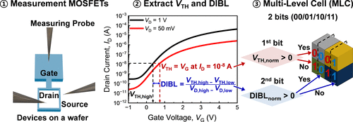
Dual-Parameter Variable Physically Unclonable Function (PUF) for Multilevel Cell Silicon MOSFETs
Sang-Min Kang - ,
Hyo-Jun Park - ,
Eui-Cheol Yun - ,
Da-Eun Bang - ,
Moon-Seok Kim *- , and
Jun-Young Park *
The rapid advancement of artificial intelligence (AI) has improved convenience but also introduced significant security risks. Physically unclonable functions (PUFs) have emerged as promising solutions to these challenges. In this study, we propose a multilevel cell (MLC)-based PUF that combines threshold voltage (VTH) and drain-induced barrier lowering (DIBL) within a single device. The statistical dependence between the two parameters was evaluated and quantified by employing conditional probabilities, entropy, mutual information (MI) and the Pearson correlation coefficient. To demonstrate this approach, single-crystalline silicon (single-Si) and polycrystalline silicon (poly-Si) channel metal oxide-semiconductor field-effect transistors (MOSFETs) were fabricated. The security of the proposed PUF was evaluated in terms of uniformity, interchip Hamming distance (HDinter), and intrachip Hamming distance (HDintra). This dual-parameter MLC scheme is compatible with monolithic integration, allowing compact cointegration of logic and security on a single chip. In particular, the poly-Si channel device supports low-temperature stacking, enabling direct integration of application processors (APs), dynamic random-access memory (DRAM), and static random-access memory (SRAM) circuits for broader system-level applicability.
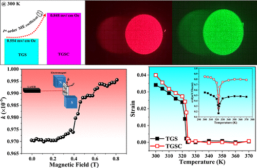
Role of Domain Dynamics in Magnetoelectric and Magneto-Optical Coupling in Triglycine Sulfate and Its Impregnated Form
Subhankar Mishra - ,
Rubina Ghosh - ,
Pujarani Swain - ,
Alok Barik - ,
Manas Ranjan Sahoo - , and
Prakash Nath Vishwakarma *
This work reports the experimental demonstration of magnetoelectric behavior in pure triglycine sulfate (TGS) and its cobalt ferrite-embedded form (TGSC). Both systems exhibit a linear magnetoelectric response, with TGSC showing ∼53% higher first-order coupling at room temperature. Strain measurement in a wide temperature range is commensurate with the observed magnetoelectricity. X-ray diffraction confirmed its phase purity, while temperature-dependent resistivity revealed contrasting thermally activated behaviors, below and above the ferroelectric–paraelectric transition temperature (obtained via dielectric measurement). Magneto-optical studies using red (633 nm) and green (532 nm) lasers revealed magnetic field-dependent modulation of transmitted intensity, with TGSC showing ∼2–2.5 times higher attenuation. Optical rotation further confirmed a magnetic field-induced enhancement of optical activity, strongly influenced by the ferrimagnetic phase. These results establish TGS and TGSC as promising magnetoelectric materials for multifunctional, field-tunable sensor and optoelectronic applications.

Anisotropic Electrical Performance of Carbon Paper Type Gas Diffusion Layers in Proton Exchange Membrane Fuel Cells
Yanqin Chen *- and
Xiaojin Li *
The electrical resistance of gas diffusion layers (GDLs) contributes a major portion of the performance losses in proton exchange membrane fuel cells (PEMFCs). The anisotropic architecture of carbon-paper-based GDLs, coupled with the channel/rib configuration of bipolar plates (BPPs), results in complex current transport behavior. Understanding the structure–property relationship between the GDL microstructure and its anisotropic electrical properties is crucial for optimizing PEMFC performance. This work investigates the 3D anisotropic electrical performance of carbon paper type GDLs in both through-plane (TP) and in-plane (IP) directions. 2D and 3D morphological characterizations reveal the fundamental conduction mechanisms. An integrated mechanical–electrical model was developed to simulate the GDL deformation and current density distribution under realistic BPP compression conditions. Notably, TP resistance exhibits pronounced pressure dependence below 1 MPa, decreasing nonlinearly from 130 to 16 mΩ for GDL-240 and from 85 to 6 mΩ for GDL-340, consistent with surface morphology-controlled conduction. After three compression cycles, the TP electrical resistance stabilizes approximately 7 mΩ under 2 MPa for GDL-240 and 4 mΩ under 4 MPa for GDL-340, with pressure plateaus indicating microstructural saturation. These findings suggest material-specific optimal assembly pressures of 2 MPa for GDL-240 and 4 MPa for GDL-340 in PEMFC applications.

Stretching-Induced Crystallinity and Oligomer Dispersion for Antistatic Biodegradable PLA Films
Fanatchanon Maneechot - ,
Tawiwat Kunthong - ,
Thanit Kertsomboon - , and
Suwabun Chirachanchai *
The development of antistatic biodegradable polymers, particularly polylactic acid (PLA), is limited by the intrinsically high electrical resistance of PLA. To address this, we introduce a branched conductive PLA oligomer terminated with an aniline pentamer, mPEI-PLA-HDI-AP, and evaluate its effectiveness as a conductive additive at 15 wt % in PLA films. The roles of uniaxial (UNS), simultaneous biaxial (SIB), and sequential biaxial (SEB) stretching in controlling chain alignment and tuning film conductivity are systematically examined. Variation of stretching rates (75 and 10 mm/s) and draw ratios (2×, 3×, and 4×) reveals that high stretching rates combined with large draw ratios promote crystallization, especially in SIB and SEB processes. These conditions yield small crystallites (<20 nm) and low cold-crystallization enthalpies (<5 J/g), as confirmed by WAXD and DSC. These structural modifications significantly reduce surface electrical resistance to as low as 108 Ω. In contrast, annealed PLA/mPEI-PLA-HDI-AP films exhibit similar crystallinity but show no improvement in resistivity, indicating that both enhanced crystalline packing and improved dispersion and orientation of the conductive PLA oligomer are essential and can be achieved through optimal stretching. Overall, this work demonstrates that combining conductive PLA-based oligomers with controlled stretching effectively reduces film resistance from ∼1010 Ω to ∼108 Ω, enabling PLA films suitable for antistatic packaging applications.

Impact of Bi Vacancies on the Polarization and Transport Properties of Bi2FeCrO6 Thin Films
Chenyue Hu *- ,
Xavier Henning - ,
Daniel Stoeffler - ,
Laurent Schlur - ,
Gilles Versini - ,
Cédric Leuvrey - ,
François Roulland - ,
U-Chan Chung - ,
Thomas Fix - ,
Aziz Dinia - ,
Mircea V. Rastei - , and
Silviu Colis *
Among ferroelectric oxides, Bi2FeCrO6 (BFCO) stands out due to its high polarization and relatively low bandgap of 1.5 eV, which make it promising for optoelectronic applications based on visible-light absorption. Its properties such as bandgap width, polarization switching bias, and imprint of the ferroelectric hysteresis loop can be largely modulated by inducing different types of defects in the structure such as Fe (Cr) antisite defects or oxygen vacancies. In this work, we demonstrate that Bi vacancies can also play a key role in the properties of epitaxial BFCO thin films grown by pulsed laser deposition. Notably, we show that increasing the deposition temperature enhances the concentration of Bi vacancies, which, in turn, significantly impacts both the transport and ferroelectric properties. The film shows a p-type character, which is consistent with density functional theory (DFT) calculations on BFCO containing Bi vacancies. In extreme cases, the lack of Bi can lead to nonmiscible highly Bi-deficient phases with high conductivities that prevent the establishment of an electric field across the film, thereby hindering its polarization control.

Revealing Phonon Bridge Effect for Amorphous vs Crystalline Metal–Silicide Layers at Si/Ti Interfaces by a Machine Learning Potential
Mayur Singh - ,
Lokanath Patra - ,
Chengyang Zhang - ,
Gregory J. MacDougall - ,
Suman Datta - ,
David G. Cahill - , and
Satish Kumar *
This publication is Open Access under the license indicated. Learn More
Metal–semiconductor interfaces play a central role in micro- and nanoelectronic devices, as heat dissipation or temperature drop across these interfaces can significantly affect device performance. Prediction of accurate thermal boundary resistance (TBR) across these interfaces, considering realistic structures and their correlation with underlying thermal transport, remains challenging. In this work, we develop a unified Neuroevolution Potential (NEP) for the Si–Ti system that accurately reproduces energies, forces, and phonon properties of bulk Si, Ti, and TiSi2 and extends naturally to interfacial environments to analyze interfacial transport. An important development over current machine-learned interatomic potentials is the capability to model complex structures at metal–semiconductor interfaces, as the NEP enables large-scale nonequilibrium molecular dynamics simulations of epitaxial Si/Ti interfaces to elucidate the effect of amorphous or crystalline silicide interfacial layers. Simulated TBRs show excellent agreement with our time-domain thermoreflectance (TDTR) measurements, validating the robustness of our predictions. Spectral analyses reveal that the amorphous TiSi2 interfacial layer helps in efficient interfacial transport when the thickness is less than 1.5 nm compared to the crystalline TiSi2 layer, due to the high spectral conductance in the 3–6 THz frequency range and also due to the opening of channels for anharmonic transport, but this trend reverses when the interfacial layer thickness increases beyond 1.5 nm. Comparison of TBRs at the Si/TiSi2 interface for different crystalline phases of TiSi2 establishes that the C54 phase has reduced TBR compared to the C49 phase, which is correlated with the difference in their phonon density of states (PDOS) overlap with Si. These results provide atomistic insight into the role of crystalline versus amorphous silicides in interfacial heat transport and demonstrate a transferable machine-learned potential for studying heat dissipation in advanced semiconductor devices.
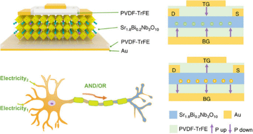
Dual-Gate-Controlled Ferroelectric Field-Effect Transistor Based on Sr1.8Bi0.2Nb3O10 Perovskite Nanosheets for a Logic Memristor
Lele Ren - ,
Minggao Zhang - ,
Junhui Tan - ,
Yunfan Wang - , and
Bao-Wen Li *
Two-dimensional (2D) perovskite ferroelectric materials have garnered significant research interest due to their large spontaneous polarization, broad operational window, and high dielectric constant, rendering them highly advantageous in nonvolatile ferroelectric memory devices. In this study, we fabricate a PVDF-TrFE dual-gate-modulated Sr1.8Bi0.2Nb3O10 (SBNO) FeFET to investigate the regulatory mechanism of PVDF-TrFE ferroelectric polarization on SBNO FeFET at the nanoscale. The fabricated device exhibits an impressive on/off ratio exceeding 106. Furthermore, we systematically examine the modulation effect of dual-gate polarization loading on the channel layer conductivity. By leveraging distinct conductive states, we successfully demonstrate the simulation of NAND logic gate operations. This work expands the application scope of ferroelectric perovskite nanosheets in multifunctional 2D ferroelectric devices.
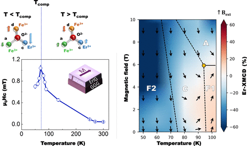
Magnetic Behavior and Phase Diagram of Epitaxial Er3Fe5O12 Thin Films across the Compensation Temperature
Satakshi Pandey *- ,
Antoine Barbier - ,
Anne Forget - ,
Brice Sarpi - ,
Francesco Maccherozzi - ,
Roberto Sant - ,
Nicholas B. Brookes - ,
Jean-Baptiste Moussy - , and
Pamella Vasconcelos Borges Pinho *
Rare-earth iron garnet (RE3Fe5O12) films are promising insulating ferrimagnets. They can show low magnetic damping, perpendicular magnetic anisotropy, and ultrafast spin dynamics, which makes them ideal for spin transport applications. In this work, we investigate the interaction between the magnetic sublattices in Er3Fe5O12 thin films grown by pulsed laser deposition on a Gd3Ga5O12 substrate. Structural and magnetic characterization reveals high-quality single-crystal growth, with a compensation temperature close to the reported bulk value (∼80 K). Magnetic phase diagrams based on element-specific measurements map out the regions where ferrimagnetic, canted, and aligned phases are stable across the compensation temperature. The micromagnetic dynamics resulting from perpendicular magnetic pulse perturbation of an in-plane magnetized layer was investigated at room temperature and revealed complex configurations. These results are key features for modulating magnetization dynamics through the compensation phenomenon, which is essential for spin-based devices operating in a low-temperature regime.
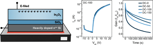
Synergistic Effects of Electric Field and Thermal Treatment on Solution-Processed In2O3 Thin-Film Transistors
Han-Lin Zhao - ,
Xiao-Lin Wang - ,
Kwan-Jun Heo - ,
Suchang Yoo - , and
Sung-Jin Kim *
Indium oxide (In2O3) thin-film transistors (TFTs) fabricated by a low-temperature solution process tend to suffer from high defect densities and poor bias stability. The introduction of a moderate direct current (DC) electric field during a brief preannealing step can provide a practical low-energy pathway to simultaneously repair structural defects and redistribute charge in the semiconductor. In2O3 films were spin-coated onto a SiO2/Si gate electrode and dielectric and subjected to a 10 V DC field for 10 min at preannealing temperatures of 0, 50, 100, and 150 °C, followed by 250 °C hard-backing. The overall performance of the device treated at 100 °C (DC-100) was the best, with a saturation mobility of 4.21 cm2 V–1 s–1 and an on/off current ratio of 8.6 × 10⁶. Long-term environmental testing showed that the on-state current dropped by only 37% after 30 days, compared to 95% for the pristine device. Gate bias stability further confirms the improved stability: under ±20 V gate stress for 400 s, the threshold voltage excursions of the DC-100 device were only 1.03 V (positive) and −0.54 V (negative), about 1/10th of the excursions observed in the original transistor. Thus, the combined thermal–electric field processing provides a scalable and straightforward solution to obtain high-mobility, bias-stabilized In2O3 TFTs.
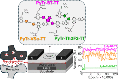
Structure–Function Coupling in Pyridyl Triazole Copolymers for Neuromorphic Synaptic Transistors
Arash Ghobadi - ,
Salahuddin Attar - ,
Abhijeet Abhi - ,
Thomas B. Kallaos - ,
Dilan M. Gamachchi - ,
Indeewari M. Karunarathne - ,
Andrew C. Meng - ,
Joseph C. Mathai - ,
Shubhra Gangopadhyay - ,
Steven P. Kelley - ,
Mohammed Al-Hashimi *- , and
Suchismita Guha *
This publication is Open Access under the license indicated. Learn More
Organic ferroelectric transistors are excellent candidates as low-cost alternatives for synaptic devices. Specifically, interfaces with donor–acceptor semiconducting polymers and copolymers of poly(vinylidene fluoride) (PVDF) are attractive for mimicking synaptic responses. By tailoring the linking unit between the pyridyl triazole (PyTr) acceptors and thiophene donors, three copolymers are synthesized incorporating selenium-substituted thiophene, benzothiadiazole, and fluorine-substituted thiophene linkers. Using the hexafluoropropylene copolymer of PVDF (PVDF-HFP) as the dielectric layer, the three PyTr semiconductors show p-type transport in transistor architectures with carrier mobilities between 0.1 and 0.2 cm2 V–1 s–1. The synaptic plasticity is investigated by applying long-term pulsed voltages at the gate electrode to emulate potentiation and depression processes. To assess their neuromorphic functionality, the synaptic responses of the devices are tested for image recognition in a multilayer perceptron neural network. The copolymer with the benzothiadiazole linker achieved recognition accuracy close to 80%, whereas the one with a fluorine-substituted thiophene linker shows no synaptic behavior, highlighting the critical role of the semiconductor–dielectric interface. A detailed study of the interface trap density and morphology is performed to identify how interfacial properties directly influence synaptic device performance.

Stabilizing Metastable Rare-Earth Ferrites on (111) Platinum via an Iron Oxide Interlayer
Marshall B. Frye - ,
Jonathan R. Chin - ,
Nicholas A. Parker - ,
Steven E. Zeltmann - ,
Matthew R. Barone - ,
Darrell G. Schlom - , and
Lauren M. Garten *
This publication is Open Access under the license indicated. Learn More
The metastable P63cm phase of ScFeO3 (h-ScFeO3) is a multiferroic material, but instability on conductive substrates limits the development of next-generation memory and magnetoelectric sensors. Unfortunately, stabilization approaches developed for insulating substrates, such as sapphire, do not translate directly to conductive substrates. In this work, we demonstrate how interlayer design preferentially stabilizes h-ScFeO3 on (111) platinum via molecular beam epitaxy while simultaneously enhancing key figures of merit. We developed a process to deposit a (111) wüstite-like interlayer with a metastable Fe3+ oxidation state to target h-ScFeO3. The films are solely (0001) oriented h-ScFeO3 without any measured secondary phases. Rocking curves of the 0004 h-ScFeO3 peak have a full width at half-maximum of 0.06°, an improvement compared to films deposited without this interlayer approach. A further indication of strain reduction in these films is structural distortion in the first layers of h-ScFeO3, overcoming the critical thickness limit in h-ScFeO3. Designing interlayers to reduce epitaxial strain and target specific phases expands the viable substrates for metastable materials and overcomes the thickness limits for improper ferroelectricity.

Skin-Inspired Flexible Dual-Mode Tactile Sensor for Material and Hardness Perception
Yuxia Li - ,
Ranran Yang - ,
Liangsong Huang - ,
Peng Zhang *- ,
Xiaofei Bu - ,
Yuteng Tang - ,
Liqun Yang - ,
Wenzheng Song - , and
Zhichao Mu
Inspired by the multireceptor collaborative perception mechanism of human skin, this study proposes a bio-inspired flexible dual-mode tactile sensor (SCTS). The sensor adopts a vertical integration strategy, combining triboelectric and capacitive pressure sensing modules into a compact thin-layer structure to simultaneously acquire material properties and pressure information. The triboelectric module, based on an electrospun polyvinylidene fluoride nanofiber membrane and laser-induced graphene electrodes, effectively captures dynamic contact signals, while the capacitive module utilizes the same electrodes with a polydimethylsiloxane dielectric layer to stably monitor static pressure. Tests demonstrate that the capacitive module achieves a detection range of 0–140 kPa with a maximum sensitivity of 0.4485 kPa–1, and the triboelectric module reliably discriminates eight common materials while maintaining consistent performance under varying pressures and frequencies. Integrated into an intelligent robotic hand system, the SCTS successfully accomplishes simultaneous identification of material type and object hardness, replicating the skin-like “fast and slow adaptation” collaborative perception mechanism. Through coordinated design of multilayer functional structures and optimization of materials and processes, this study provides a feasible approach to balancing device integration, sensitivity, and structural compactness in multimode tactile perception, demonstrating promising potential in the fields of electronic skin and intelligent robotics.
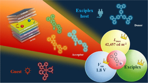
Molecular Design of Bipolar Acceptors for Ultra-Low Voltage and High-Luminance Red PhOLEDs Based on DPQ Derivatives
Yu-Ru Yang - ,
Kuan-Yu Su - ,
Pei-Yu Lai - ,
Yi-Jhan Huang - ,
Ting-Hsuan Chuang - ,
Chin-Wei Lu *- , and
Chih-Hao Chang *
This publication is Open Access under the license indicated. Learn More
The rational design of host materials with intrinsic bipolar characteristics is critical for achieving high-performance phosphorescent organic light-emitting diodes (PhOLEDs). In this work, three diphenylquinoxaline (DPQ) derivatives functionalized with cyano (−CN), phenylcarbazole, and dibenzofuran groups were developed as versatile acceptors and paired with tris(4-carbazoyl-9-ylphenyl)amine (TCTA) as an electron donor. All acceptors exhibited well-balanced carrier-transport properties and optimized energy-level alignment. Among them, the TCTA:DPQCN-PhDBF exciplex host system achieved outstanding performance, delivering an ultralow turn-on voltage (Von) of 1.8 V, the lowest reported to date, along with a maximum luminance (Lmax) of 42,457 cd m–2 and a peak external quantum efficiency (EQEmax) of 16.8%. The superior performance is attributed to extended π-conjugation, increased molecular torsion, and the rigid dibenzofuran unit, which collectively enhance charge-transfer (CT) state formation, hole-transport efficiency, film morphology stability, and energy-level modulation. In comparison, DPQCN-DBF exhibited limited performance due to crystallization tendencies during film formation, whereas the TCTA:DPQCN-CzPh system achieved a high EQEmax of 17.8% with a low Von of 2.0 V, benefiting from improved hole-transport properties imparted by the carbazole unit. This study establishes a systematic molecular design strategy that integrates energy-level tuning, charge-transport balancing, and CT-state optimization, offering valuable insights for the development of high-efficiency, high-luminance, and energy-saving OLED technologies.
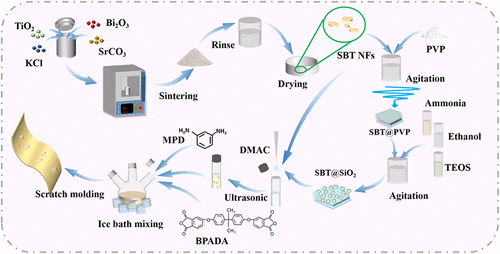
Special Two-Dimensional Structure of Strontium Bismuth Titanate Nanosheets Enhancing Energy Storage Performance and High-Temperature Stability of Polymer Dielectrics
Mengge Zhao - ,
Ziyue Wang - ,
Haiping Xu *- ,
Hongfei Li *- ,
Yiming Gao - ,
Bin Cheng - ,
Huaqing Xie - ,
Wei Xiong - , and
Shuaifei Zhao
In advanced electronics and power systems, flexible dielectric materials with a high energy density are crucial. To compensate for the low dielectric constant (εr) and insufficient energy storage density of polymer materials, inorganic fillers with high εr, typically zero- or one-dimensional, are commonly introduced. However, 0D fillers, like nanoparticles, tend to agglomerate in the polymer matrix, increasing interfacial defects and exacerbating polarization losses, whereas 1D fillers, such as nanotubes and nanowires, can disrupt flexibility and mechanical properties due to their high aspect ratios and poor interfacial compatibility. In contrast, two-dimensional (2D) nanosheets, with excellent thickness-to-diameter ratios, can interact more effectively with the polymer matrix, reducing interfacial polarization, enhancing dispersion, and improving interface compatibility. Furthermore, these 2D nanosheets can serve as conductive barriers, limiting charge migration and hindering the expansion of electrical trees, thereby significantly improving the stability and service life of composite materials. This study synthesized bismuth strontium titanate (SrBi4Ti4O15, abbreviated as SBT) nanosheets with distinct two-dimensional structure, excellent temperature stability, and low dielectric loss using a simple and cost-effective molten salt method. SBT/poly(ether imide) (PEI) composite films were then prepared by an in situ polymerization process. Experimental results show that the 0.5 vol % SBT/PEI composite films exhibit an energy storage density of 6.69 J/cm3 and a charge–discharge efficiency of 94.09% at room temperature while maintaining stable dielectric properties across the 0–200 °C temperature range. To further enhance interfacial compatibility, we synthesized SBT@SiO2 core–shell nanoflakes. With the same filler loading, the energy storage density of the composite films increased to 8.37 J/cm3, with a charge–discharge efficiency of 92.46%. This work provides an idea for the fabrication of high-energy-density polymer nanocomposites.

High-Strength and Weavable Smart Nanoyarn Fabric for Unconstrained Ballistocardiogram Monitoring in Home Settings
Pan Liu - ,
Xinyu Geng - ,
Lianrui Liang - ,
Hang Wang - ,
Xuyan Lu *- , and
Mingwei Tian *
Long-term, comfortable sleep monitoring is essential for maintaining good health, identifying sleep disorders, and preventing chronic diseases. However, the current gold standard, polysomnography (PSG), is impractical for prolonged use due to its reliance on multiple wired physiological sensors, which interfere with natural sleep patterns, as well as its high operational costs. Respiratory and cardiac signals are key parameters for sleep monitoring, and ballistocardiogram (BCG) are physical signals generated with cardiac activity, which can be monitored in an unconstrained way. Herein, a flexible piezoelectric fabric sensor based on polyvinylidene fluoride (PVDF) yarn is developed for unconstrained physiological signal monitoring. The sensor exhibited a tensile strength over 150 MPa, an operational stability of 10000 loading cycles, and a sensitivity of 34 mV/kPa, enabling it to detect subtle vibration signals such as respiration and BCG. Benefiting from the woven architecture of the yarns, the fabric’s durability and comfort are comparable to those of standard bed linens. The sensor enables nonintrusive monitoring of BCG signals even under high static pressure, demonstrating significant potential for long-term home sleep monitoring and personalized health management.
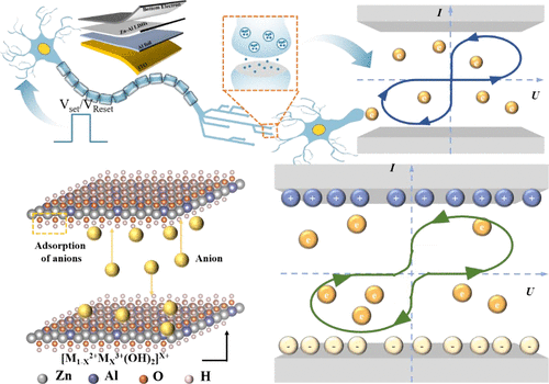
Unveiling Capacitive Coupling and Dynamic Modulation of Memristive Switching in Zn–Al Layered Double Hydroxide Films
Dong Li - ,
Shaojie Zhang - ,
Luyang Ge - ,
Jiangtao Pan - ,
Xiyan Bao - ,
Qian Zhang - ,
Junqing Huang - ,
Kunkun Cao - ,
Guokun Ma - ,
Yiheng Rao - ,
Jun Zhang *- ,
Houzhao Wan *- , and
Hao Wang *
To address the demand for rapid, high-density information storage, memristors have garnered significant research interest owing to their structural simplicity, rapid switching speed, and low power consumption. Layered double hydroxides (LDHs), a class of two-dimensional materials, show promise for emerging neuromorphic applications. In this work, we fabricated Zn–Al LDH thin-film memristive devices using a low-cost synthesis route. This layered structure exhibits a unique coupling between capacitive and resistive switching behaviors. Notably, the devices demonstrate sustained current retention even after external bias removal, enabling simultaneous memristive and memcapacitive functionalities. The Zn–Al LDH thin-film memristor (1 μm) exhibits a switching ratio exceeding 10 at a low operating voltage of 0.7 V. Crucially, the device demonstrates robust endurance, maintaining stable switching over 300 write/erase cycles with highly uniform and reproducible hysteresis characteristics. Furthermore, external stimuli (e.g., voltage) induce reversible transitions between capacitively coupled memristive states and pure memristive operation. This capability enhances the feasibility of implementing second-order associative memory circuits, as these neuromorphic devices inherently mimic neural network structures. Consequently, it expands the application potential for “self-generated” memory within neural network architectures.
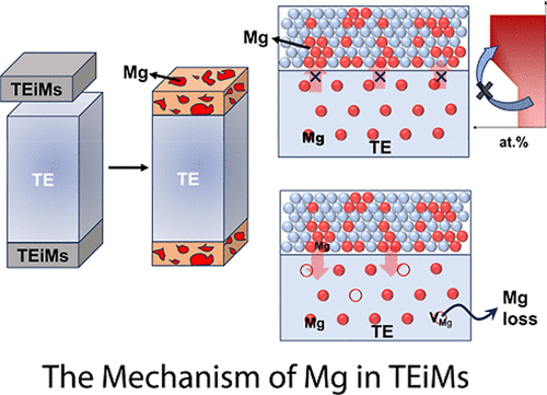
Effect of Elemental Magnesium on the Interfacial Thermal Stability of Mg3Sb1.5Bi0.5-Based Thermoelectric Devices
Shiqiang Yan - ,
Kezhang Zhang - ,
Zhenyang Qi - ,
Qiang Zhang - ,
Wenhao Fan - , and
Shaoping Chen *
Thermoelectric technology converts low-grade waste heat into electrical energy, offering an environmentally sustainable pathway for global development. N-type Mg3(Sb, Bi)2 thermoelectric materials have garnered significant attention due to their outstanding thermoelectric performance over broad temperatures (27–500 °C). However, unavoidable Mg loss and interfacial element diffusion degrade the performance and service life of thermoelectric devices, thereby limiting the application of thermoelectric technology. Here, we introduce elemental Mg into thermoelectric interfacial materials (TEiMs) to suppress harmful Mg diffusion and compensate for Mg loss within the material, achieving dual stability in Mg3(Sb, Bi)2 devices. After 30 days of aging, Mg3(Sb, Bi)2 single-arm devices maintained an outstanding power density of 0.75 W/cm2 and a remarkable conversion efficiency of 8.9%, demonstrating unprecedented stability. These findings offer design strategies for TEiMs and provide valuable references for interface engineering in diverse thermoelectric systems, thereby advancing the practical feasibility of thermoelectric energy harvesting in renewable energy and waste heat applications.
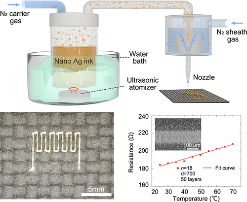
Fabrication and Optimization of Aerosol-Jet-Printed Temperature Sensors on Carbon Fiber-Reinforced Composites
Jian Wang - ,
Guangyin Yu - ,
Jinqiang Ai - ,
Honghao Li - ,
Linyuan Sun - ,
Zikun Lin - ,
Yangyi Deng - ,
Shaoming Luo - ,
Feng Gu - ,
Yumei Zhou *- , and
Fenglin Zhang *
Carbon fiber-reinforced composite (CFRP) exhibits high specific strength and excellent fatigue resistance, demonstrating broad application prospects. Direct fabrication of microscale sensors on CFRP surfaces has significant implications for structural health monitoring and functional integration. However, fabricating sensors on CFRP remains challenging due to its inherently weak surface polarity, while existing printedcircuit technologies suffer from low resolution and complex procedures. In this work, a temperature sensor was fabricated directly on CFRP via pretreatment, aerosol jet printing (AJP), and sintering. High-precision Ag nanoparticles (AgNPs) traces were printed by optimizing the printing parameters (carrier/sheath gas flow rate and printing speed) through simulation and experimental analysis. Then, AgNPs circuits with good conductivity and adhesion performance were obtained by optimizing the sintering processes, such as sintering temperature and time. Finally, grid temperature sensors with a temperature coefficient of resistance (TCR) of 2.981 × 10⁻³/°C and a resistance change rate of 0.545 Ω·°C–1 were successfully fabricated. The sensor achieved precise temperature sensing over 25 ∼ 70 °C with a response time of less than 200 ms and retained good stability after 500 cyclic operation tests, demonstrating excellent temperature monitoring capability. This work demonstrates advanced sensor fabrication on CFRP, paving the way for its potential applications in microelectronics, sensing, and monitoring.

Ab Initio Quantum Transport Simulations of the Sub-3 nm Gate-Length Monolayer CuBr Transistors for High-Performance Device Applications
Mudasser Husain - ,
Younas Ahmed - ,
Xingyue Yang - ,
Zongmeng Yang - ,
Jiahui Li - ,
Jichao Dong - ,
Linqiang Xu - ,
Nasir Rahman - ,
Shibo Fang - , and
Jing Lu *
As the physical thickness of silicon decreases, the effective carrier mobility (μ) degrades significantly, leading to a substantial reduction in the performance of field-effect transistors (FETs). In this context, two-dimensional (2D) semiconductors have emerged as promising channel materials for next-generation transistors owing to their atomic-scale thickness and intrinsically high carrier mobility. In 2D materials, monolayer (ML) CuBr exhibits an atomic-layer thickness similar to graphene and demonstrates carrier mobilities of 1153.54 cm2 V–1 s–1 for electrons (μe) and 15.88 cm2 V–1 s–1 for holes (μh), which are higher than those of many other 2D semiconductors, such as MoS2 (∼200 cm2 V–1 s–1) and BN (∼487 cm2 V–1 s–1). Leveraging the atomic-scale thickness with high electron mobility of ML-CuBr, we performed quantum transport simulations to evaluate the performance limits of the sub-3 nm gate-length (Lg) double-gated (DG) n-type FETs for high-performance (HP) device applications. Our simulation results show that the ML-CuBr n-type FETs outperform the requirements set by the international technology roadmap for semiconductors (ITRS) for the 2028 horizon technology node. Notably, at Lg = 3 nm, the device demonstrates high Ion of 1372 μA/μm, ultralow subthreshold swing (SS) of 45 mV/dec, transconductance (gm) of 5.62 mS/μm, time-delay (τ) of 0.337 ps, power-delay product (PDP) of 0.246 fJ/μm, and energy-delay product (EDP) of 8.29 × 10⁻²⁹ Js/μm. These findings establish ML-CuBr as a highly promising channel material capable of enabling ultrascaled, energy-efficient transistors for high-performance device applications.
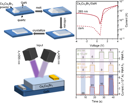
Melt-Crystallized Ultrawide-Bandgap Cs3Cu2Br5 Films for Self-Powered Dual-Band Deep-UV/Near-UV Photodetection
Xiaopeng Huang - ,
Sheng Ma - ,
Jiaquan Li - ,
Huimin Duan - ,
Hainan Qin - ,
Xiaobing Cao - ,
Xin He - ,
Yiming Sun *- ,
Shuti Li *- , and
Weidong Song *
Cesium–copper halide Cs3Cu2Br5 has recently emerged as a promising ultrawide-bandgap semiconductor for deep-ultraviolet (DUV) photodetection owing to its excellent optical characteristics and environmental robustness. Nevertheless, achieving high-quality Cs3Cu2Br5 films remains difficult, as solution- or vapor-phase processes typically yield small grains, high defect densities, and poor compactness that severely limit device performance. Herein, we introduce a capillary-driven molten-precursor transport strategy combined with supercooling-controlled melt crystallization to fabricate dense Cs3Cu2Br5 polycrystalline films. By optimizing the degree of undercooling, it enables the formation of large grains (average grain area reaches 1.5 × 104 μm2) with minimal porosity and few grain boundaries, microstructural features surpassing those reported previously. On this basis, self-powered Cs3Cu2Br5/GaN heterojunction photodetectors were realized, exhibiting a distinct dual-band photoresponse within the DUV and near-UV (NUV) regions. At 265 nm, the device achieves an on/off ratio of 1.45 × 10³ and a specific detectivity of 1.3 × 10⁹ Jones, together with a fast transient response and excellent operational stability. Furthermore, a proof-of-concept encrypted optical communication scheme was demonstrated by exploiting the detectors’ wavelength selectivity for enhanced transmission security. This work establishes an effective approach for fabricating high-quality Cs3Cu2Br5 films and highlights their potential in DUV/NUV dual-band photodetection for secure optoelectronic systems.
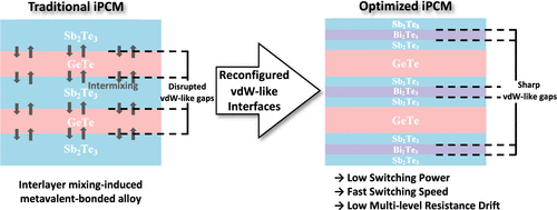
Reconfiguration of van der Waals-like Interface in Superlattice Phase Change Material for Data Storage and Computing
Xixi Zou - ,
Ruobing Wang - ,
Yuqing Chen - ,
Ziqi Wan - ,
Sannian Song - ,
Yulai Zhu - ,
Yanping Sui - ,
Tianjiao Xin - ,
Zhitang Song *- , and
Xilin Zhou *
Superlattice phase change memory, composed of alternately stacked crystalline phase change layers of Sb2Te3 and GeTe (GeTe/Sb2Te3), significantly reduces the switching energy and time by restricting atomic movement during the phase transition process. To further enhance the switching performance of the memory device, this study proposes a sandwich structure consisting of Sb2Te3/Bi2Te3/Sb2Te3 (ST/BT/ST) layers, achieved by reconfiguring the van der Waals-like interface, to replace the Sb2Te3 layer of traditional GeTe/Sb2Te3 superlattice phase change material. A highly textured GeTe/ST/BT/ST superlattice film is deposited using a back-end-of-line-compatible sputtering technique, resulting in sharp van der Waals-like interfaces. Electrical switching measurements of a prototype device incorporating the ST/BT/ST structure demonstrate a reduced switching voltage and enhanced stability across multiple resistance levels, accompanied by low resistance drift. Electrothermal simulations indicate that the observed low-power switching behavior arises from the material’s low thermal conductivity and reduced thermal dissipation within the sandwiched superlattice. These findings suggest that the proposed superlattice phase change material holds significant promise for applications in low-power data storage and non-von Neumann computing devices.

A Partially Ion-Exchanged Perovskite Single-Crystal Heterojunction for Self-Powered Photodetection
Zhen Yu Zhang *- and
Guo Ping Wang *
Heterojunctions, characterized by built-in electric fields and efficient charge-carrier separation, represent a promising architecture for high-performance perovskite photodetectors (PDs). Unlike traditional template methods, the confined ion-exchange strategy described here operates directly on high-quality single-crystal (SC) wafers, offering significant technical advantages for heterojunction device fabrication. Leveraging spatial confinement effects, this method enables precise component gradient regulation while effectively circumventing the interface defects and structural damage typically associated with template synthesis and postremoval processes. Notably, this approach features strong process compatibility, allowing seamless integration with existing semiconductor technologies, and high system universality, making it applicable to diverse perovskite systems. Under a forward bias of 5 V, the resulting heterojunction PD exhibits good performance, with a responsivity (R) of 9.9 A/W, specific detectivity (D) of 2.58 × 10¹² Jones, external quantum efficiency (EQE) of 3038%, and linear dynamic response (LDR) of 109.2 dB. Even under self-powered conditions, the PD maintains R of 0.143 A/W, D of 2.21 × 10¹¹ Jones, EQE of 43%, and LDR of 102.7 dB. The confined ion-exchange method proposed herein provides a universal solution with significant potential for the large-scale chemical preparation of heterojunction devices.

Room-Temperature High-Performance InP/Si Surface-Activated Wafer Bonding for Electronic-Photonic System Integration Applications
Changlin Wu - ,
Jieqiong Zhang *- ,
Hei Wong *- ,
Jun Liu - ,
Xiao Qin - ,
Lichao Wu - ,
Wenhan Bao - ,
Junhui Duan - ,
Bo Zhao - ,
Anli Yang - , and
Xu Chen
Indium phosphide (InP)–silicon wafer bonding, which offers both high performance and fabrication efficiency at reduced cost, is widely regarded as a key enabler for next-generation electronic–photonic integrated circuits (EPICs). Among the available approaches, surface-activated bonding (SAB) has emerged as a particularly promising technique. Nevertheless, the bonding interface still faces significant challenges, as its mechanical strength, electrical conductivity, and thermal performance fall short of the desired standards. In this work, we introduce a proprietary in situ surface cleaning and activation process in conjunction with an ultrahigh-vacuum wafer bonding system to achieve robust InP/Si bonding at room temperature. A tensile strength of 3 MPa was obtained, sufficient to withstand mechanical stresses produced during subsequent front-end device fabrication processes. Following a brief low-temperature thermal treatment at 300 °C, readily available with many standard IC fabrication processes, the bonding strength exceeded 7 MPa, reaching the strongest InP bonding achieved with plasma-activated bonding (PAB). High-resolution TEM revealed a void-free, ordered interfacial layer less than 3 nm thick. X-ray diffraction (XRD) and energy-dispersive spectroscopy (EDS) were employed to evaluate crystallinity, stress uniformity, and oxygen/phosphorus distribution in the thinner and more vulnerable InP wafers. We discovered that Ar plasma cleaning and surface activation promote InP oxidation, degrading material properties. To mitigate this, alternative approaches such as employing larger ions (e.g., Xe) and reducing plasma energy are proposed. For the first time, current conduction mechanisms across the bonded interface are reported and suggested as a characterization tool for probing electrical and defect properties of the cross-wafer pn junction. These findings provide effective strategies for process optimization, enhancing both mechanical integrity and electrical reliability of bonded InP wafers, and underscore the potential of the proposed bonding approach to advance heterogeneous integration in future EPIC technologies.
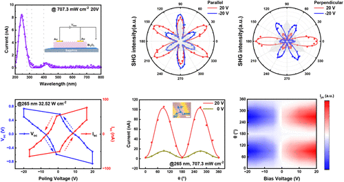
Ferroelectric Bi2O3 Nanoflakes for a High Polarization Ratio in UVC Photodetectors
Runhui Wang - ,
Wei Ying - ,
Xin Wang - ,
Yan Zhang - ,
Ying Liu *- , and
Shujie Tang *
Low-dimensional ferroelectrics with wide bandgaps demonstrate great potential in realizing high-contrast polarimetric ultraviolet-C (UVC) photodetectors. However, numerous UVC platforms suffer from limited polarization discrimination, and their polar-order signatures may diminish at elevated temperatures, thereby hindering robust polarimetric readout. Here, we report rhombohedral ferroelectric Bi2O3 nanoflakes synthesized via a pressure-induced flux-assisted growth method, with a noncentrosymmetric second-harmonic generation (SHG) response observed up to ∼750 K. Cross-sectional low-loss electron energy-loss spectroscopy (EELS) yields an optical bandgap of 3.96 eV, and wavelength-dependent photoresponse measurements show a pronounced UVC response with strongly suppressed response at longer wavelengths, supporting solar-blind operation. Poling-dependent photovoltaic I–V switching and bias-tunable polarization-resolved SHG collectively indicate a correlation between the enhanced photocurrent and the switchable polar state, consistent with the bias-tunable SHG symmetry response. Consequently, an electrically tunable polarization ratio is achieved. Planar Au/Bi2O3/Au photodetectors exhibit polarization-resolved UVC photoresponse at 265 nm with a polarization ratio up to 42.7 and reversible photocurrent polarity upon reversing the poling direction, allowing a switchable sign of the polarization-dependent photoresponse. These results highlight Bi2O3 nanoflakes as a wide-bandgap polar platform for electrically tunable polarization-sensitive UVC optoelectronics.

Tuning Structural, Electronic, and Optical Properties of α-In2Se3 by an External Electric Field
Maolin Zeng - ,
Lu Li *- ,
Pei Zhang - ,
Zhao Zhang - ,
Ze Xue - ,
Qixiang Yin - ,
Delin Wei - ,
Shengshi Liu - , and
Qiyi Zhao *
The various polymorphic structures of ferroelectric semiconductors contribute to distinct electronic properties. Fully researching the mechanisms of phase transitions and controlling these phases through external stimuli offers a promising route to tailor the material’s optoelectronic behaviors and provides ideas for the development of functional devices. In this paper, the phase transition of In2Se3 and related optoelectronic properties under the condition of an electric field are investigated systematically, from two complementary aspects: the field-driven structural transition mechanism in the bulk and the optical response modulation in monolayer systems relevant to two-dimensional device scales. The results show that applying an in-plane electric field of 0.05–0.20 V Å–1 rearranges the Se-4p orbitals and promotes electron transitions, inducing the migration of Se2– ions as well as interlayer sliding and the progressive evolution of the local coordination environment, thereby triggering the transformation from the α phase to the β phase in In2Se3. This field-induced α–β phase transition reveals the strong coupling between lattice polarization and electronic structure in In2Se3, providing microscopic insight into the interplay between electric-field control and structural stability in ferroelectric layered materials. Building on this mechanism, we further quantify in monolayer α-In2Se3 how the electric field modulates the band-edge positions and the linear optical response. Furthermore, second-harmonic generation measurements reveal exceptionally large nonlinear coefficients, with the out-of-plane d33 exceeding 103 pm V–1, confirming their strong potential for infrared-to-visible frequency conversion. This work clarifies the microscopic mechanism of electric-field-driven phase transitions in In2Se3, demonstrating a practical route for tuning its electronic and optical responses as well as providing a basis for the design of phase-change optoelectronic devices.

In Situ Formation of Silver Trifluoroacetate-Doped, Highly Conductive, Dual-Functional Poly(3-hexylthiophene) Nanowire Networks during Spin Coating for Self-Powered Photodetectors
Hyeyoung Kim - ,
Seongeun Oh - ,
Se Hun Joo *- , and
Minwoo Park *
Photodetectors (PDs) play crucial roles in various optoelectronic applications. Metal oxide/organic semiconductor junction-based PDs are particularly promising because they exhibit excellent responsivity, detectivity, and fast broadband response. Among conductive polymers, polythiophenes are good candidates for use as light absorbers and hole-transport layers in PDs owing to their facile thin-film processability and robust environmental stability. However, achieving high conductivity remains challenging, primarily because of their intrinsically low carrier density and limited crystallinity. These characteristics directly affect charge-transfer efficiency and overall device performance. In this study, we introduced silver trifluoroacetate (AgTFA) as a hole dopant for poly(3-hexylthiophene) (P3HT), leading to the formation of highly dense nanowire networks during spin coating. The high solubility of AgTFA in aromatic solvents enabled strong coordination between Ag+ ions and thiophene units, promoting π–π stacking along the [010] direction. Furthermore, efficient Ag+ doping significantly enhanced the conductivity from 8.71 × 10⁻⁴ to 8.11 S cm–1. The underlying doping and nanowire formation mechanisms were elucidated using density functional theory calculations, which identified the optimized doping sites. SnO2, deposited by atomic layer deposition, served as both light absorber and electron transport layers. Interestingly, the roles of SnO2 and P3HT interchanged depending on the wavelength, with ultraviolet and visible light primarily absorbed in SnO2 and P3HT, respectively. Owing to the enhanced conductivity of P3HT, the resulting PDs exhibited outstanding responsivity (32.9–104.6 mA W–1), detectivity (4.58 × 10¹²–1.21 × 10¹³ Jones), and external quantum efficiency (8.75%–43.26%), comparable to those of high-performance organic and perovskite PDs.

Room-Temperature Ferroelectric LaMnO3: Supercritical CO2-Induced Lattice Strain and Jahn–Teller Distortion
Bo Gao - ,
Mingzhu Tan - ,
Song Xu - ,
Wenzhuo Wu - ,
Qingyong Tian - ,
Huanhuan Yang - , and
Qun Xu *
Ferroelectric materials are regarded as core functional materials for next-generation information storage and energy-conversion devices, yet achieving stable ferroelectric performance at room temperature remains a significant challenge. In this study, supercritical CO2 was employed to facilitate the selective incorporation of CO2 molecules into oxygen vacancies in LaMnO3, accompanied by partial repair of the oxygen vacancies, thereby introducing local lattice strain and structural bias. This strain propagates throughout the material via long-range elastic interactions, ultimately disrupting the global lattice symmetry and successfully stabilizing the room-temperature ferroelectric phase. Experiments demonstrate a significant positive correlation between the degree of lattice strain and the efficiency of oxygen-vacancy repair. The optimal sample exhibits excellent ferroelectric performance, with a maximum polarization intensity approximately 30 times higher than that of the original sample. Based on experimental characterization and theoretical calculations, this study reveals that structural bias modulates the local crystal field to drive noncentrosymmetric orbital ordering, which in turn induces Jahn–Teller distortion and polar structural distortion, ultimately stabilizing the ferroelectric Pmc21 phase. This discovery not only provides a theoretical perspective for understanding the microscopic origin of ferroelectricity in perovskite oxides but also lays a scientific foundation for designing room-temperature ferroelectric materials through chemical-incorporation strategies.
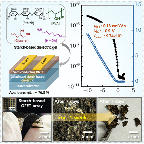
A Fully Starch-Based Platform Moving beyond Partial Eco-Friendliness for System-Level Biodegradable Organic Electronics
Hyekyeong Kim - ,
Dineshkumar Mani - ,
Taehoon Hwang - ,
Jisu Park - ,
Yumin Kim - ,
Hyunseo Jang - ,
Seongbin Kim - , and
Hwa Sung Lee *
Eco-friendly, disposable organic electronics require device stacks composed of biodegradable components to ensure genuine environmental viability at end-of-life. Although bioderived materials have been investigated extensively, many reported systems remain “partially green,” as practical stacks often retain nondegradable elements or processing steps that are misaligned with eco-friendly disposal. Here, a solution-processed platform that moves beyond these limitations is demonstrated by utilizing starch as both the transparent substrate and the dielectric, strengthening comprehensive system-level eco-friendliness. The starch-based composite dielectric is fabricated via aqueous gelatinization incorporating a minimal amount of poly(vinyl alcohol) binder, glycerol plasticizer, and hexamethylenediamine (HMDA) cross-linker. Morphological analyses confirm that the combined incorporation of glycerol and HMDA markedly reduces surface roughness and suppresses drying-induced microcracks, yielding mechanically resilient and morphologically uniform dielectric films. Bottom-gate organic transistors exhibit well-defined p-type behavior with an on/off current ratio of 9.7 × 10⁵, a stabilized threshold voltage of approximately −0.9 V, and a field-effect mobility of 0.21 cm2 V–1 s–1 (averaged over ≥10 devices per formulation). Biodegradation tests verify end-of-life compatibility, as starch-based devices undergo rapid structural disintegration within 7 days of soil burial. These results establish starch-based composites as a practical, scalable route toward truly disposable organic electronics.
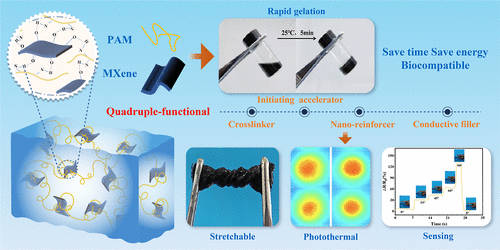
Quadruple-Functional MXene Enables Ultrafast, Green Fabrication of High-Performance Polyacrylamide Hydrogels for Flexible Strain Sensors
Xiaoling Yang - ,
Xiaofang Wang - ,
Yuhao Hu - ,
Huimin Xiang - ,
Congyan Xia - ,
Xiaoling Liao - ,
Yuanyuan Zhang *- ,
Maolan Zhang *- , and
Ming Zhou *
Polyacrylamide (PAM) hydrogels are promising candidates for flexible wearable sensors but suffer from limitations including toxic cross-linkers(N,N′-methylenebis(acrylamide), BIS), prolonged gelation times, high-temperature requirements, and inadequate mechanical properties. Herein, a quadruple-functional MXene was employed to fabricate high-performance PAM hydrogels within 5 min at ambient temperature. MXenes served simultaneously as an initiating accelerator (replacing toxic BIS), physical cross-linker, conductive agent, and reinforcing nanofiller. Reductive MXene nanosheets catalyzed ultrafast polymerization of acrylamide monomers via redox reactions with ammonium persulfate(APS), facilitating a green, low-energy fabrication process and preventing MXene nanosheets reaggregation within the hydrogel network. By adjusting the MXene content, the optimized hydrogel (6 mg/mL MXene) demonstrated exceptional mechanical performance, with 1558% elongation at break and 119 kPa tensile strength, exceeding traditional BIS/PAM hydrogels (1081% elongation, 74 kPa strength). This enhancement is attributed to the uniform honeycomb-like porous structure and dual-network architecture comprising covalent PAM backbone and physical hydrogen-bonded MXene cross-links. Additionally, the MXene incorporation confers electrical conductivity (0.3 S/m) and photothermal performance, with temperature increase up to 21.8 °C under near-infrared (NIR) irradiation and good photothermal stability. As a strain sensor, the hydrogel exhibits two-stage sensing response with gauge factor (GF) of 1.1 (0–235%) and 2.4 (235–400%), rapid response time (35 ms), recovery time (98 ms), and excellent cyclic stability. In L929 cytotoxicity assays, MXene/PAM hydrogels demonstrate improved biocompatibility compared to BIS/PAM hydrogels. The sensor accurately monitors both large human movements (finger, wrist, bending, handwriting) and subtle physiological activities (pulse and throat vibrations). This study introduces a rapid, eco-friendly method for fabricating multifunctional PAM hydrogels with enhanced mechanical, conductive, photothermal, and biocompatible properties for flexible electronic skin and biomedical devices.
In Situ Growth of Two-Dimensional Crystalline/Amorphous NiO Heterojunction as an Excellent Electrode Material for Supercapacitors
Yingjing Liu - ,
Shuting Han - ,
Yinfeng Wang - ,
Xiuguang Yi - ,
Xiaojiao Wu - ,
Lina Yang - ,
Litong Zhao - ,
Xuexia Liu *- , and
Zhijun Wang *
NiO nanomaterials have been extensively employed as electrode materials for supercapacitors, owing to their economic viability and ease of fabrication. However, low energy density and poor cycling stability of NiO nanomaterials hinder their application in the energy storage field. Herein, two-dimensional crystalline/amorphous NiO/carbon cloth (2D NiO/CC) nanosheets have been synthesized via a facile hydrothermal and thermal treatment method. When used as electrode materials for supercapacitors, NiO/CC exhibits a specific capacitance of 121.82 F cm–2 at 1 mA cm–2, along with a Coulombic efficiency of nearly 100% and a remarkable capacity retention of 150.83% after 10,000 charging/discharging cycles. In conclusion, the present study not only offers insights into the study of NiO nanomaterials but also highlights their significant potential for energy storage applications.

Engineering Field-Like Spin Torques with Sign Reversal Using a Fe3GeTe2 Insertion Layer
Ziqian Cui - ,
Qianwen Zhao - ,
Jiahe Yu - ,
Qi Wang - ,
Tianxiao Zhu - ,
Hanying Zhang - , and
Chong Bi *
Current-induced spin–orbit torque (SOT) provides an efficient electrical approach to manipulate magnetization in spintronic devices, where most research has focused on the enhancement of damping-like (DL)-SOT. However, field-like (FL)-SOT, which has been proven to dominate ultrafast (subnanosecond) in-plane magnetization manipulation, has received relatively little attention. Here, we demonstrate robust FL-SOT modulation, even with sign reversal, by engineering SOT-material/ferromagnet interfaces in typical Pt/CoFeB SOT bilayers through an Fe3GeTe2 insertion layer. Our results indicate that FL-SOT can be modulated by a factor of 2 with sign reversal, while DL-SOT is also modulated but consistently retains the same sign. Furthermore, control samples with an additional Cu insertion layer confirm that the independent modulation and sign reversal of FL-SOT are determined by the proximity-induced interfacial ferromagnetism via the Fe3GeTe2 insertion layer, which alters spin scattering at the Pt/CoFeB interfaces. This work provides an effective pathway for precisely tailoring the often-neglected FL-SOT, which is crucial for developing ultrafast SOT devices.

Balancing Both Coercivity and Magnetization in Compositionally Graded Ru:LSMO Epitaxial Thin Films: A Separate Analysis of Surface/Interface and Bulk Magnetism by a Complementary Approach
Gaku Sato - ,
Kenichi Kaminaga *- ,
Takayasu Hanashima - ,
Kazuhiro Akutsu-Suyama - ,
Tetsuro Ueno - ,
Yoshiyuki Ohtsubo - ,
Yuto Abiko - ,
Ryota Kimura - ,
Keita Sasaki - ,
Hibiki Murakami - ,
Keisuke Haruki - ,
Ayumu Kikuchi - ,
Rintaro Kimura - ,
Hiroshi Naganuma - ,
Shingo Maruyama - ,
Hiroyuki Aoki - , and
Yuji Matsumoto
This publication is Open Access under the license indicated. Learn More
Compositionally graded profiles of a substituent element artificially introduced into a complex oxide can offer a viable route to decouple and retune physical properties in a trade-off relationship caused by uniform substitution. Here, this is demonstrated with particular attention to the magnetism in Ru-substituted LSMO ((La,Sr)(Mn,Ru)O3) epitaxial films with the Ru composition linearly increasing (UP-graded) or decreasing (DOWN-graded) along the growth direction. A combination of macroscopic magnetometry and depth-resolved polarized neutron reflectometry (PNR) allows for the magnetism of surface/interface and the in-between bulk layer to be separately discussed to reveal how the introduction of a composition gradient has solved the trade-off among Curie temperature (TC), saturation magnetization (Ms), and coercivity (Hc) in Ru-substituted LSMO. Macroscopically graded films exhibit as much enhancement in Hc as the corresponding uniformly substituted films, with TC and Ms, which otherwise will be monotonically reduced, being maintained as high as the unsubstituted film. In an UP-graded film, the surface and interface magnetization is more strongly suppressed than that in the uniformly substituted films, while the Ms in the in-between bulk layer is found to be microscopically graded according to the local Ru composition. Importantly, despite the suppression in magnetization at the interface and surface, each local magnetization in the in-between bulk layer is higher than that of its uniform counterpart. As a result, the UP-graded LSMO yields higher magnetization than the corresponding uniformly substituted film, consistent with the macroscopic magnetometry result. Bulk-sensitive Mn L2,3-edge fluorescence-yield X-ray magnetic circular dichroism (XMCD) of the UP-graded film further provides evidence that the Mn spin sublattice is genuinely responsible for the magnetic enhancement by the Ru composition gradient. The present successful balancing of TC, Ms, and Hc in LSMO will reinforce the possibility of LSMO as a spintronic oxide material, encouraging further exploration of potential applications of the compositionally graded profiling approach in other related oxide systems.
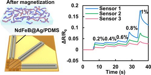
Triaxial Flexible Multifunctional Strain Sensors Based on Self-Assembled NdFeB@Ag Magnetic Conductive Composites
Miaoning Ren - ,
Qiushuo Wu - ,
Zhen Yang - ,
Yang Qin - , and
Xian Huang *
Conventional strain sensors are single function and struggle to meet the demands of applications in dynamic, complex environments. This paper presents the design, fabrication, and application of a triaxial flexible strain sensor based on magnetized neodymium iron boron microparticles with silver nanoshells (NdFeB@Ag) embedded in PDMS. Magnetized NdFeB@Ag microparticles with strong magnetism and high conductivity self-assemble to form conductive networks, facilitating efficient and scalable fabrication via stencil printing. A parylene encapsulation layer ensures long-term signal stability by mitigating moisture and oxidation effects, reducing the resistance drift in unmagnetized NdFeB@Ag/PDMS composites to just 7.7% over 12 h. The resulting strain sensor demonstrates excellent multifunctionality, with the ability to detect strain within the range of 0–1% in three orthogonal directions, monitor bending angles from 0° to 90°, and respond to temperature changes within the range of 25–45 °C due to its positive temperature coefficient. This research based on NdFeB@Ag magnetic conductive microparticles presents a convenient approach to construct multifunctional strain sensors, leading to a prevalence of low-cost devices in soft robotics, wearable electronics, and intelligent home systems.

Excellent Stability of n-Type Thermoelectric Thin Films Using Cationic Surfactant/Single-Walled Carbon Nanotube Composites
Kento Sunaga - ,
Asumi Eguchi - ,
Yoshiyuki Shinozaki - ,
Shuya Ochiai - ,
Keisuke Uchida - ,
Sachiko Aida-Hyugaji - , and
Masayuki Takashiri *
Single-walled carbon nanotubes (SWCNTs) are promising for thermoelectric generators (TEGs) in IoT applications; however, the long-term instability of the n-type properties remains a significant challenge. This study systematically investigates the factors governing n-type stability in SWCNT films combined with cationic surfactants featuring different halide counterions: DODMAC (Cl–), DODMAB (Br–), and DODMAI (I–). Through a combination of experimental characterization and molecular dynamics (MD) simulations, we demonstrate that all SWCNT films mixed with the surfactant films remain stable n-type for more than 280 days, with Seebeck coefficients of approximately −50 μV/K. MD simulations and XPS depth profiling reveal that the cationic surfactants form a dense adsorption layer that acts as a robust physical barrier─a “bulk encapsulation”─effectively shielding the SWCNTs from oxygen infiltration. While Seebeck stability was consistent across all surfactants, electrical conductivity was found to depend on the counterion species, with DODMAC exhibiting the highest performance due to its dense bundle packing. These findings elucidate the synergistic mechanism of electronic doping and physical shielding, providing crucial design guidelines for the development of highly stable n-type SWCNT thermoelectric materials.
Mastheads
Issue Editorial Masthead

This publication is free to access through this site. Learn More
Issue Publication Information
This publication is free to access through this site. Learn More