


This publication is Open Access under the license indicated. Learn More

ACS Editors' Choice® is a collection designed to feature scientific articles of broad public interest. Read the latest articles
Mechanical Detuning of Exciton–Phonon Resonance in WS2Click to copy article linkArticle link copied!
- Álvaro Rodríguez*Álvaro Rodríguez*Email: [email protected]Instituto de Ciencia de Materiales de Madrid (ICMM-CSIC), C. Sor Juana Inés de la Cruz 3, 28049 Madrid, SpainMore by Álvaro Rodríguez
- Carmen MunueraCarmen MunueraInstituto de Ciencia de Materiales de Madrid (ICMM-CSIC), C. Sor Juana Inés de la Cruz 3, 28049 Madrid, SpainMore by Carmen Munuera
- Andres Castellanos-GomezAndres Castellanos-GomezInstituto de Ciencia de Materiales de Madrid (ICMM-CSIC), C. Sor Juana Inés de la Cruz 3, 28049 Madrid, SpainMore by Andres Castellanos-Gomez
ACS Photonics
© 2026 The Authors. Published by American Chemical Society. This publication is licensed under
License Summary*
You are free to share (copy and redistribute) this article in any medium or format and to adapt (remix, transform, and build upon) the material for any purpose, even commercially within the parameters below:

Creative Commons (CC): This is a Creative Commons license.

Attribution (BY): Credit must be given to the creator.
*Disclaimer
This summary highlights only some of the key features and terms of the actual license. It is not a license and has no legal value. Carefully review the actual license before using these materials.
Abstract
Controlling resonant Raman scattering in two-dimensional semiconductors typically requires tuning the excitation energy to match excitonic transitions. Here we show that mechanical deformation can achieve the same effect without changing the laser energy, enabling a controlled transition between resonant and nonresonant Raman scattering at fixed excitation. By applying biaxial strain of up to 1.3% to WS2, the B exciton is red-shifted by 180 meV. This large excitonic shift leads to a pronounced collapse of the double-resonant 2LA(M) mode under 532 nm excitation, quantitatively described by a resonance model formulated in terms of the B exciton energy. Meanwhile, first-order phonons remain narrow and reversible, confirming elastic deformation and efficient strain transfer. These results establish mechanical strain as an effective knob to control exciton–phonon-mediated light–matter interactions. They enable deterministic and reversible tuning of resonance-enhanced Raman scattering and excitonic optical responses in layered semiconductors.
This publication is licensed under
License Summary*
You are free to share(copy and redistribute) this article in any medium or format and to adapt(remix, transform, and build upon) the material for any purpose, even commercially within the parameters below:
Creative Commons (CC): This is a Creative Commons license.
Attribution (BY): Credit must be given to the creator.
*Disclaimer
This summary highlights only some of the key features and terms of the actual license. It is not a license and has no legal value. Carefully review the actual license before using these materials.
Introduction
Results and Discussion
Experimental Configuration and Strain Calibration
Figure 1
Figure 1. Experimental configuration and strain calibration. (a) Photograph of the cross-shaped flexible polycarbonate (PC) substrate used to apply biaxial strain. The central region hosts the large WS2 layers, and mechanical strain is applied along yellow arrows. (b) Optical micrograph of the WS2 monolayer, bilayer, and trilayer regions on Au/PC. Scale bar is 10 μm. (c) Pillar-array calibration of the biaxial strain. Optical images collected before and after bending at 2% strain reveal isotropic expansion of pillar spacing. (d) Strain extracted from pillar displacements as a function of Z-stage position (Z). The linear fit (ε = kZ) provides the calibration used throughout this work.
Resonant Raman Response of Trilayer WS2
Figure 2
Figure 2. Resonant Raman features in trilayer WS2 under 532 nm excitation. (a) Raman spectrum at zero strain (ε = 0%) showing the resonant enhancement of the 2LA(M) band. The spectral decomposition highlights contributions from the E, A1, and 2LA(M) modes obtained by multipeak fitting (Voigt profiles). Peak labels and colors match those used in the strain-dependent measurements. Overlap between the E phonon and the double-resonant 2LA(M) mode produces an asymmetric band whose intensity and shape are highly sensitive to exciton-mediated resonance. (b) Schematic representation of the double-resonant 2LA(M) Raman process. An optical excitation near K is followed by two intervalley scattering events mediated by LA phonons with wavevectors ±q close to M, before radiative recombination. This mechanism underlies the strong resonance sensitivity of the 2LA(M) feature.
Transition from Resonant to Nonresonant Raman Scattering under Strain
Figure 3
Figure 3. Phonon softening and resonant Raman evolution in biaxially strained WS2. (a) Raman spectra of trilayer WS2 acquired at increasing biaxial strain. (b) Strain dependence of the E, A1, and 2LA(M) phonon frequencies. Linear fits yield slopes of −6.8 ± 0.10, −2.3 ± 0.08, and −10.8 ± 0.6 cm–1/%, respectively. Using , we obtain the Grüneisen parameter for each Raman mode: γ(E) = 0.96 ± 0.05, γ(A1) = 0.28 ± 0.03, and γ(2LA) = 1.54 ± 0.15. (c) Zoomed view of the spectra highlighting red shifts and the reduction of resonant enhancement.
Exciton Shifts under Biaxial Strain
Figure 4
Figure 4. Differential-reflectance tracking of exciton energies under biaxial strain. (a) Normalized ΔR/R spectra showing the systematic red shift of the A and B excitons with increasing tensile biaxial strain. Purple and orange arrows indicate the A trion (XAT) and exciton (XA) positions, respectively. The background signal was subtracted from each spectrum for clarity. (b) Strain dependence of the XA, XB, and XAT energies. Linear fits yield a slope of −138.6 ± 10 meV/% for the B exciton, corresponding to a total shift of ∼−180 meV at ε = 1.3%. The green line marks the laser excitation energy (EL).
Strain-Driven Suppression of Double-Resonant 2LA(M) Scattering
Figure 5
Figure 5. Strain-controlled transition between resonant and nonresonant 2LA(M) scattering. (a) B-exciton energy as a function of biaxial strain extracted from differential reflectance. The green horizontal line indicates the fixed laser excitation energy (2.33 eV). (b) Strain dependence of the E and 2LA(M) Raman modes positions. (c) Normalized intensity of the 2LA(M) as a function of B-exciton energy, showing a continuous suppression as the exciton is shifted away from resonance with the laser (green line). The upper horizontal axis indicates the corresponding biaxial strain. The purple solid line represents the effective resonance model used to quantify the detuning-dependent decay of the 2LA(M) intensity.
Exciton-Mediated Resonance Model
Conclusion
Supporting Information
The Supporting Information is available free of charge at https://pubs.acs.org/doi/10.1021/acsphotonics.5c03089.
Experimental methods, images of the experimental biaxial setup, AFM images of the samples, spatial uniformity of the applied biaxial strain, additional Raman datasets for monolayer and bilayer WS2, raw data of differential reflectance spectra, experiments demonstrating the reversibility of the applied strain under biaxial strain, and details of the theoretical detuning model (PDF)
Terms & Conditions
Most electronic Supporting Information files are available without a subscription to ACS Web Editions. Such files may be downloaded by article for research use (if there is a public use license linked to the relevant article, that license may permit other uses). Permission may be obtained from ACS for other uses through requests via the RightsLink permission system: http://pubs.acs.org/page/copyright/permissions.html.
Author Information
- Andres Castellanos-Gomez - Instituto de Ciencia de Materiales de Madrid (ICMM-CSIC), C. Sor Juana Inés de la Cruz 3, 28049 Madrid, Spain;
 https://orcid.org/0000-0002-3384-3405
Á.R. conceived the study, fabricated the samples, carried out the experiments, and performed the data analysis. C.M. and A.C.-G. supervised the project and provided guidance on data interpretation and conceptual development. Á.R. wrote the manuscript with input and critical feedback from both coauthors. All of the authors approved the final version of the manuscript.
Á.R. acknowledges funding from the European Union under Marie Skłodowska-Curie Grant Agreement 101109987. A.C-G. and C.M. acknowledge support from Grants PDC2023-145920-I00 and PID2023-151946OB-I00, funded by MICIU/AEI/10.13039/501100011033 and respectively by the European Union NextGenerationEU/PRTR (PDC2023-145920-I00) and ERDF/EU (PID2023-151946OB-I00). A.C.-G. also acknowledges funding from the European Research Council (ERC) through the ERC-PoC 2024 StEnSo Project (Grant Agreement 101185235) and the ERC-2024 SyG SKIN2DTRONICS Project (Grant Agreement 101167218). ICMM-CSIC authors acknowledge support from the Severo Ochoa Centres of Excellence Program through Grant CEX2024-001445-S, funded by MICIU/AEI/10.13039/501100011033.
References
This article references 52 other publications.
- 1Niehues, I.; Schmidt, R.; Drüppel, M.; Marauhn, P.; Christiansen, D.; Selig, M.; Berghäuser, G.; Wigger, D.; Schneider, R.; Braasch, L.; Koch, R.; Castellanos-Gomez, A.; Kuhn, T.; Knorr, A.; Malic, E.; Rohlfing, M.; Michaelis de Vasconcellos, S.; Bratschitsch, R. Strain Control of Exciton-Phonon Coupling in Atomically Thin Semiconductors. Nano Lett. 2018, 18 (3), 1751– 1757, DOI: 10.1021/acs.nanolett.7b04868Google ScholarThere is no corresponding record for this reference.
- 2Wang, G.; Chernikov, A.; Glazov, M. M.; Heinz, T. F.; Marie, X.; Amand, T.; Urbaszek, B. Colloquium: Excitons in Atomically Thin Transition Metal Dichalcogenides. Rev. Mod. Phys. 2018, 90 (2), 021001, DOI: 10.1103/RevModPhys.90.021001Google ScholarThere is no corresponding record for this reference.
- 3Brem, S.; Ekman, A.; Christiansen, D.; Katsch, F.; Selig, M.; Robert, C.; Marie, X.; Urbaszek, B.; Knorr, A.; Malic, E. Phonon-Assisted Photoluminescence from Indirect Excitons in Monolayers of Transition-Metal Dichalcogenides. Nano Lett. 2020, 20 (4), 2849– 2856, DOI: 10.1021/acs.nanolett.0c00633Google ScholarThere is no corresponding record for this reference.
- 4Dadgar, A. M.; Scullion, D.; Kang, K.; Esposito, D.; Yang, E. H.; Herman, I. P.; Pimenta, M. A.; Santos, E.-J. G.; Pasupathy, A. N. Strain Engineering and Raman Spectroscopy of Monolayer Transition Metal Dichalcogenides. Chem. Mater. 2018, 30 (15), 5148– 5155, DOI: 10.1021/acs.chemmater.8b01672Google ScholarThere is no corresponding record for this reference.
- 5Peng, Z.; Chen, X.; Fan, Y.; Srolovitz, D. J.; Lei, D. Strain Engineering of 2D Semiconductors and Graphene: From Strain Fields to Band-Structure Tuning and Photonic Applications. Light: Sci. Appl. 2020, 9 (1), 190, DOI: 10.1038/s41377-020-00421-5Google ScholarThere is no corresponding record for this reference.
- 6Hernández López, P.; Heeg, S.; Schattauer, C.; Kovalchuk, S.; Kumar, A.; Bock, D. J.; Kirchhof, J. N.; Höfer, B.; Greben, K.; Yagodkin, D.; Linhart, L.; Libisch, F.; Bolotin, K. I. Strain Control of Hybridization between Dark and Localized Excitons in a 2D Semiconductor. Nat. Commun. 2022, 13 (1), 7691, DOI: 10.1038/s41467-022-35352-9Google ScholarThere is no corresponding record for this reference.
- 7Kumar, A. M.; Yagodkin, D.; Rosati, R.; Bock, D. J.; Schattauer, C.; Tobisch, S.; Hagel, J.; Höfer, B.; Kirchhof, J. N.; Hernández López, P.; Burfeindt, K.; Heeg, S.; Gahl, C.; Libisch, F.; Malic, E.; Bolotin, K. I. Strain Fingerprinting of Exciton Valley Character in 2D Semiconductors. Nat. Commun. 2024, 15 (1), 7546, DOI: 10.1038/s41467-024-51195-yGoogle ScholarThere is no corresponding record for this reference.
- 8Ronco, G.; Martínez-Suárez, A.; Tedeschi, D.; Savaresi, M.; Hierro-Rodríguez, A.; McVitie, S.; Stroj, S.; Aberl, J.; Brehm, M.; García-Suárez, V. M.; Rota, M. B.; Alonso-González, P.; Martín-Sánchez, J.; Trotta, R. Strain-Induced Exciton Redistribution among Quantum Emitters in Two-Dimensional Materials. npj 2D Mater. Appl. 2025, 9 (1), 65, DOI: 10.1038/s41699-025-00588-8Google ScholarThere is no corresponding record for this reference.
- 9Negi, D.; Baishya, M.; Moghe, A. R.; Paul, S.; Badola, S.; Saha, S. Uniaxial Strain-Dependent Resonant Raman Scattering in WS2. Small 2025, 21 (17), 2412832, DOI: 10.1002/smll.202412832Google ScholarThere is no corresponding record for this reference.
- 10Carrascoso, F.; Frisenda, R.; Castellanos-Gomez, A. Biaxial versus Uniaxial Strain Tuning of Single-Layer MoS2. Nano Mater. Sci. 2022, 4 (1), 44– 51, DOI: 10.1016/j.nanoms.2021.03.001Google ScholarThere is no corresponding record for this reference.
- 11Kourmoulakis, G.; Michail, A.; Paradisanos, I.; Marie, X.; Glazov, M. M.; Jorissen, B.; Covaci, L.; Stratakis, E.; Papagelis, K.; Parthenios, J.; Kioseoglou, G. Biaxial Strain Tuning of Exciton Energy and Polarization in Monolayer WS2. Appl. Phys. Lett. 2023, 123 (22), 223103, DOI: 10.1063/5.0167724Google ScholarThere is no corresponding record for this reference.
- 12Michail, A.; Anestopoulos, D.; Delikoukos, N.; Grammatikopoulos, S.; Tsirkas, S. A.; Lathiotakis, N. N.; Frank, O.; Filintoglou, K.; Parthenios, J.; Papagelis, K. Tuning the Photoluminescence and Raman Response of Single-Layer WS2 Crystals Using Biaxial Strain. J. Phys. Chem. C 2023, 127 (7), 3506– 3515, DOI: 10.1021/acs.jpcc.2c06933Google ScholarThere is no corresponding record for this reference.
- 13Yang, J. A.; Bennett, R. K. A.; Hoang, L.; Zhang, Z.; Thompson, K. J.; Michail, A.; Parthenios, J.; Papagelis, K.; Mannix, A. J.; Pop, E. Biaxial Tensile Strain Enhances Electron Mobility of Monolayer Transition Metal Dichalcogenides. ACS Nano 2024, 18 (28), 18151– 18159, DOI: 10.1021/acsnano.3c08996Google ScholarThere is no corresponding record for this reference.
- 14Oliva, R.; Wozniak, T.; Faria, P. E. J.; Dybala, F.; Kopaczek, J.; Fabian, J.; Scharoch, P.; Kudrawiec, R. Strong Substrate Strain Effects in Multilayered WS2 Revealed by High-Pressure Optical Measurements. ACS Appl. Mater. Interfaces 2022, 14 (17), 19857– 19868, DOI: 10.1021/acsami.2c01726Google ScholarThere is no corresponding record for this reference.
- 15Gastaldo, M.; Varillas, J.; Rodríguez, Á.; Velický, M.; Frank, O.; Kalbáč, M. Tunable Strain and Bandgap in Subcritical-Sized MoS2 Nanobubbles. npj 2D Mater. Appl. 2023, 7 (1), 71, DOI: 10.1038/s41699-023-00432-xGoogle ScholarThere is no corresponding record for this reference.
- 16Henríquez-Guerra, E.; Li, H.; Pasqués-Gramage, P.; Gosálbez-Martínez, D.; D’Agosta, R.; Castellanos-Gomez, A.; Calvo, M. R. Large Biaxial Compressive Strain Tuning of Neutral and Charged Excitons in Single-Layer Transition Metal Dichalcogenides. ACS Appl. Mater. Interfaces 2023, 15 (49), 57369– 57378, DOI: 10.1021/acsami.3c13281Google ScholarThere is no corresponding record for this reference.
- 17Manzanares-Negro, Y.; Zambudio, A.; López-Polín, G.; Sarkar, S.; Chhowalla, M.; Gómez-Herrero, J.; Gómez-Navarro, C. Fatigue Response of MoS2 with Controlled Introduction of Atomic Vacancies. Nano Lett. 2023, 23 (23), 10731– 10738, DOI: 10.1021/acs.nanolett.3c02479Google ScholarThere is no corresponding record for this reference.
- 18Stellino, E.; D’Alò, B.; Blundo, E.; Postorino, P.; Polimeni, A. Fine-Tuning of the Excitonic Response in Monolayer WS2 Domes via Coupled Pressure and Strain Variation. Nano Lett. 2024, 24 (13), 3945– 3951, DOI: 10.1021/acs.nanolett.4c00157Google ScholarThere is no corresponding record for this reference.
- 19Polimeno, L.; Di Renzo, A.; Manoccio, M. C.; Mastria, R.; De Giorgi, M.; Esposito, M.; Rizzo, A.; De Marco, L.; Ballarini, D.; Tasco, V.; Dominici, L.; Sanvitto, D.; Todisco, F. Energy Control of Strain-Induced Localized States in a WS2 Monolayer. Opt. Express 2025, 33 (25), 53165– 53172, DOI: 10.1364/OE.563119Google ScholarThere is no corresponding record for this reference.
- 20Marchiani, D.; Jimenez-Arevalo, N.; Rago, I.; Pandolfi, F.; Cavoto, G.; Sbroscia, M.; Dudin, P.; Avila, J.; Mariani, C.; Betti, M. G.; Frisenda, R. Tensile Strain-Induced Bandgap Reduction and Exciton Recombination in a Trilayer MoS2 Nanosheet Wrinkle: Implications for Nanoscale Optoelectronic and Photonic Devices. ACS Appl. Nano Mater. 2025, 8 (42), 20230– 20238, DOI: 10.1021/acsanm.5c02997Google ScholarThere is no corresponding record for this reference.
- 21Harats, M. G.; Kirchhof, J. N.; Qiao, M.; Greben, K.; Bolotin, K. I. Dynamics and Efficient Conversion of Excitons to Trions in Non-Uniformly Strained Monolayer WS2. Nat. Photonics 2020, 14 (5), 324– 329, DOI: 10.1038/s41566-019-0581-5Google ScholarThere is no corresponding record for this reference.
- 22Rodriguez, A.; Kalbáč, M.; Frank, O. Strong Localization Effects in the Photoluminescence of Transition Metal Dichalcogenide Heterobilayers. 2D Mater. 2021, 8 (2), 025028, DOI: 10.1088/2053-1583/abe363Google ScholarThere is no corresponding record for this reference.
- 23Roy, S.; Yang, X.; Gao, J. Biaxial Strain Tuned Upconversion Photoluminescence of Monolayer WS2. Sci. Rep. 2024, 14 (1), 3860, DOI: 10.1038/s41598-024-54185-8Google ScholarThere is no corresponding record for this reference.
- 24Waheed, Y.; Shit, S.; Surendran, J. T.; Prasad, I. D.; Watanabe, K.; Taniguchi, T.; Kumar, S. Large Trion Binding Energy in Monolayer WS2 via Strain-Enhanced Electron-Phonon Coupling. Commun. Mater. 2025, 6 (1), 86, DOI: 10.1038/s43246-025-00809-zGoogle ScholarThere is no corresponding record for this reference.
- 25Rodríguez, Á.; Çakıroğlu, O.; Li, H.; Carrascoso, F.; Mompean, F.; Garcia-Hernandez, M.; Munuera, C.; Castellanos-Gomez, A. Improved Strain Transfer Efficiency in Large-Area Two-Dimensional MoS2 Obtained by Gold-Assisted Exfoliation. J. Phys. Chem. Lett. 2024, 15 (24), 6355– 6362, DOI: 10.1021/acs.jpclett.4c00855Google ScholarThere is no corresponding record for this reference.
- 26Androulidakis, C.; Koukaras, E. N.; Parthenios, J.; Kalosakas, G.; Papagelis, K.; Galiotis, C. Graphene Flakes under Controlled Biaxial Deformation. Sci. Rep. 2016, 5 (1), 18219, DOI: 10.1038/srep18219Google ScholarThere is no corresponding record for this reference.
- 27Michail, A.; Anestopoulos, D.; Delikoukos, N.; Parthenios, J.; Grammatikopoulos, S.; Tsirkas, S. A.; Lathiotakis, N. N.; Frank, O.; Filintoglou, K.; Papagelis, K. Biaxial Strain Engineering of CVD and Exfoliated Single- and Bi-Layer MoS2 Crystals. 2D Mater. 2021, 8 (1), 015023, DOI: 10.1088/2053-1583/abc2deGoogle ScholarThere is no corresponding record for this reference.
- 28Magda, G. Z.; Pető, J.; Dobrik, G.; Hwang, C.; Biró, L. P.; Tapasztó, L. Exfoliation of Large-Area Transition Metal Chalcogenide Single Layers. Sci. Rep. 2015, 5 (1), 14714, DOI: 10.1038/srep14714Google ScholarThere is no corresponding record for this reference.
- 29Velický, M.; Donnelly, G. E.; Hendren, W. R.; McFarland, S.; Scullion, D.; DeBenedetti, W. J. I.; Correa, G. C.; Han, Y.; Wain, A. J.; Hines, M. A.; Muller, D. A.; Novoselov, K. S.; Abruña, H. D.; Bowman, R. M.; Santos, E. J. G.; Huang, F. Mechanism of Gold-Assisted Exfoliation of Centimeter-Sized Transition-Metal Dichalcogenide Monolayers. ACS Nano 2018, 12 (10), 10463– 10472, DOI: 10.1021/acsnano.8b06101Google ScholarThere is no corresponding record for this reference.
- 30Velický, M.; Rodriguez, A.; Bouša, M.; Krayev, A. V.; Vondráček, M.; Honolka, J.; Ahmadi, M.; Donnelly, G. E.; Huang, F.; Abruña, H. D.; Novoselov, K. S.; Frank, O. Strain and Charge Doping Fingerprints of the Strong Interaction between Monolayer MoS2 and Gold. J. Phys. Chem. Lett. 2020, 11 (15), 6112– 6118, DOI: 10.1021/acs.jpclett.0c01287Google ScholarThere is no corresponding record for this reference.
- 31Rodriguez, A.; Velický, M.; Řáhová, J.; Zólyomi, V.; Koltai, J.; Kalbáč, M.; Frank, O. Activation of Raman Modes in Monolayer Transition Metal Dichalcogenides through Strong Interaction with Gold. Phys. Rev. B 2022, 105 (19), 195413, DOI: 10.1103/PhysRevB.105.195413Google ScholarThere is no corresponding record for this reference.
- 32Zhao, W.; Ghorannevis, Z.; Amara, K. K.; Pang, J. R.; Toh, M.; Zhang, X.; Kloc, C.; Tan, P. H.; Eda, G. Lattice Dynamics in Mono- and Few-Layer Sheets of WS2 and WSe2. Nanoscale 2013, 5 (20), 9677– 9683, DOI: 10.1039/c3nr03052kGoogle ScholarThere is no corresponding record for this reference.
- 33del Corro, E.; Botello-Méndez, A.; Gillet, Y.; Elias, A. L.; Terrones, H.; Feng, S.; Fantini, C.; Rhodes, D.; Pradhan, N.; Balicas, L.; Gonze, X.; Charlier, J.-C.; Terrones, M.; Pimenta, M. A. Atypical Exciton-Phonon Interactions in WS2 and WSe2 Monolayers Revealed by Resonance Raman Spectroscopy. Nano Lett. 2016, 16 (4), 2363– 2368, DOI: 10.1021/acs.nanolett.5b05096Google ScholarThere is no corresponding record for this reference.
- 34Molas, M. R.; Nogajewski, K.; Potemski, M.; Babiński, A. Raman Scattering Excitation Spectroscopy of Monolayer WS2. Sci. Rep. 2017, 7 (1), 5036, DOI: 10.1038/s41598-017-05367-0Google ScholarThere is no corresponding record for this reference.
- 35Liu, H.-L.; Yang, T.; Tatsumi, Y.; Zhang, Y.; Dong, B.; Guo, H.; Zhang, Z.; Kumamoto, Y.; Li, M.-Y.; Li, L.-J.; Saito, R.; Kawata, S. Deep-Ultraviolet Raman Scattering Spectroscopy of Monolayer WS2. Sci. Rep. 2018, 8 (1), 11398, DOI: 10.1038/s41598-018-29587-0Google ScholarThere is no corresponding record for this reference.
- 36Berkdemir, A.; Gutiérrez, H. R.; Botello-Méndez, A. R.; Perea-López, N.; Elías, A. L.; Chia, C.-I.; Wang, B.; Crespi, V. H.; López-Urías, F.; Charlier, J.-C.; Terrones, H.; Terrones, M. Identification of Individual and Few Layers of WS2 Using Raman Spectroscopy. Sci. Rep. 2013, 3 (1), 1755, DOI: 10.1038/srep01755Google ScholarThere is no corresponding record for this reference.
- 37Chen, S.-Y.; Zheng, C.; Fuhrer, M. S.; Yan, J. Helicity-Resolved Raman Scattering of MoS2, MoSe2, WS2, and WSe2 Atomic Layers. Nano Lett. 2015, 15 (4), 2526– 2532, DOI: 10.1021/acs.nanolett.5b00092Google ScholarThere is no corresponding record for this reference.
- 38Carvalho, B. R.; Wang, Y.; Mignuzzi, S.; Roy, D.; Terrones, M.; Fantini, C.; Crespi, V. H.; Malard, L. M.; Pimenta, M. A. Intervalley Scattering by Acoustic Phonons in Two-Dimensional MoS2 Revealed by Double-Resonance Raman Spectroscopy. Nat. Commun. 2017, 8 (1), 14670, DOI: 10.1038/ncomms14670Google ScholarThere is no corresponding record for this reference.
- 39Mohiuddin, T. M. G.; Lombardo, A.; Nair, R. R.; Bonetti, A.; Savini, G.; Jalil, R.; Bonini, N.; Basko, D. M.; Galiotis, C.; Marzari, N.; Novoselov, K. S.; Geim, A. K.; Ferrari, A. C. Uniaxial Strain in Graphene by Raman Spectroscopy: $G$ Peak Splitting, Gr\″uneisen Parameters, and Sample Orientation. Phys. Rev. B 2009, 79 (20), 205433, DOI: 10.1103/PhysRevB.79.205433Google ScholarThere is no corresponding record for this reference.
- 40del Corro, E.; de la Roza, A. O.; Taravillo, M.; Baonza, V. G. Raman Modes and Grüneisen Parameters of Graphite under Compressive Biaxial Stress. Carbon N. Y. 2012, 50 (12), 4600– 4606, DOI: 10.1016/j.carbon.2012.05.046Google ScholarThere is no corresponding record for this reference.
- 41Chernikov, A.; Berkelbach, T. C.; Hill, H. M.; Rigosi, A.; Li, Y.; Aslan, B.; Reichman, D. R.; Hybertsen, M. S.; Heinz, T. F. Exciton Binding Energy and Nonhydrogenic Rydberg Series in Monolayer WS2. Phys. Rev. Lett. 2014, 113 (7), 76802, DOI: 10.1103/PhysRevLett.113.076802Google ScholarThere is no corresponding record for this reference.
- 42Raja, A.; Chaves, A.; Yu, J.; Arefe, G.; Hill, H. M.; Rigosi, A. F.; Berkelbach, T. C.; Nagler, P.; Schüller, C.; Korn, T.; Nuckolls, C.; Hone, J.; Brus, L. E.; Heinz, T. F.; Reichman, D. R.; Chernikov, A. Coulomb Engineering of the Bandgap and Excitons in Two-Dimensional Materials. Nat. Commun. 2017, 8 (1), 15251, DOI: 10.1038/ncomms15251Google ScholarThere is no corresponding record for this reference.
- 43Carrascoso, F.; Lin, D.-Y.; Frisenda, R.; Castellanos-Gomez, A. Biaxial Strain Tuning of Interlayer Excitons in Bilayer MoS2. J. Phys. Mater. 2020, 3 (1), 015003, DOI: 10.1088/2515-7639/ab4432Google ScholarThere is no corresponding record for this reference.
- 44Frisenda, R.; Drüppel, M.; Schmidt, R.; Michaelis de Vasconcellos, S.; Perez de Lara, D.; Bratschitsch, R.; Rohlfing, M.; Castellanos-Gomez, A. Biaxial Strain Tuning of the Optical Properties of Single-Layer Transition Metal Dichalcogenides. npj 2D Mater. Appl. 2017, 1 (1), 10, DOI: 10.1038/s41699-017-0013-7Google ScholarThere is no corresponding record for this reference.
- 45Zollner, K.; Junior, P. E. F.; Fabian, J. Strain-Tunable Orbital, Spin-Orbit, and Optical Properties of Monolayer Transition-Metal Dichalcogenides. Phys. Rev. B 2019, 100 (19), 195126, DOI: 10.1103/PhysRevB.100.195126Google ScholarThere is no corresponding record for this reference.
- 46He, K.; Poole, C.; Mak, K. F.; Shan, J. Experimental Demonstration of Continuous Electronic Structure Tuning via Strain in Atomically Thin MoS2. Nano Lett. 2013, 13 (6), 2931– 2936, DOI: 10.1021/nl4013166Google ScholarThere is no corresponding record for this reference.
- 47Conley, H. J.; Wang, B.; Ziegler, J. I.; Haglund, R. F. J.; Pantelides, S. T.; Bolotin, K. I. Bandgap Engineering of Strained Monolayer and Bilayer MoS2. Nano Lett. 2013, 13 (8), 3626– 3630, DOI: 10.1021/nl4014748Google ScholarThere is no corresponding record for this reference.
- 48Castellanos-Gomez, A.; Roldán, R.; Cappelluti, E.; Buscema, M.; Guinea, F.; van der Zant, H. S. J.; Steele, G. A. Local Strain Engineering in Atomically Thin MoS2. Nano Lett. 2013, 13 (11), 5361– 5366, DOI: 10.1021/nl402875mGoogle ScholarThere is no corresponding record for this reference.
- 49Lemos, J. S.; Blundo, E.; Polimeni, A.; Pimenta, M. A.; Righi, A. Exciton-Phonon Interactions in Strained Domes of Monolayer MoS2 Studied by Resonance Raman Spectroscopy. Nanomaterials. 2023, 13, 2722, DOI: 10.3390/nano13192722Google ScholarThere is no corresponding record for this reference.
- 50Soubelet, P.; Bruchhausen, A. E.; Fainstein, A.; Nogajewski, K.; Faugeras, C. Resonance Effects in the Raman Scattering of Monolayer and Few-Layer MoSe2. Phys. Rev. B 2016, 93 (15), 155407, DOI: 10.1103/PhysRevB.93.155407Google ScholarThere is no corresponding record for this reference.
- 51Shi, L.; Rohringer, P.; Wanko, M.; Rubio, A.; Waßerroth, S.; Reich, S.; Cambré, S.; Wenseleers, W.; Ayala, P.; Pichler, T. Electronic Band Gaps of Confined Linear Carbon Chains Ranging from Polyyne to Carbyne. Phys. Rev. Mater. 2017, 1 (7), 075601, DOI: 10.1103/PhysRevMaterials.1.075601Google ScholarThere is no corresponding record for this reference.
- 52Heeg, S.; Shi, L.; Pichler, T.; Novotny, L. Raman Resonance Profile of an Individual Confined Long Linear Carbon Chain. Carbon N. Y. 2018, 139, 581– 585, DOI: 10.1016/j.carbon.2018.07.007Google ScholarThere is no corresponding record for this reference.
Cited By
This article has not yet been cited by other publications.

ACS Photonics
© 2026 The Authors. Published by American Chemical Society. This publication is licensed under
License Summary*
You are free to share (copy and redistribute) this article in any medium or format and to adapt (remix, transform, and build upon) the material for any purpose, even commercially within the parameters below:
Creative Commons (CC): This is a Creative Commons license.
Attribution (BY): Credit must be given to the creator.
*Disclaimer
This summary highlights only some of the key features and terms of the actual license. It is not a license and has no legal value. Carefully review the actual license before using these materials.
Article Views
Altmetric
Citations
Article Views are the COUNTER-compliant sum of full text article downloads since November 2008 (both PDF and HTML) across all institutions and individuals. These metrics are regularly updated to reflect usage leading up to the last few days.
Citations are the number of other articles citing this article, calculated by Crossref and updated daily. Find more information about Crossref citation counts.
The Altmetric Attention Score is a quantitative measure of the attention that a research article has received online. Clicking on the donut icon will load a page at altmetric.com with additional details about the score and the social media presence for the given article. Find more information on the Altmetric Attention Score and how the score is calculated.
Recommended Articles
Abstract
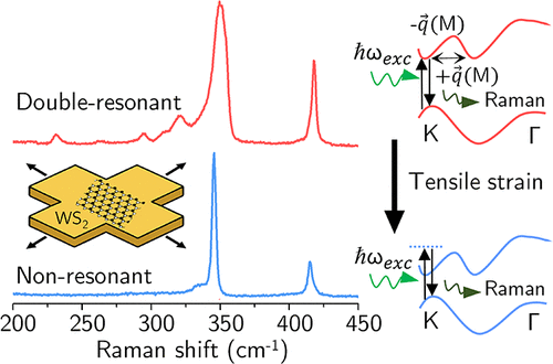
Figure 1

Figure 1. Experimental configuration and strain calibration. (a) Photograph of the cross-shaped flexible polycarbonate (PC) substrate used to apply biaxial strain. The central region hosts the large WS2 layers, and mechanical strain is applied along yellow arrows. (b) Optical micrograph of the WS2 monolayer, bilayer, and trilayer regions on Au/PC. Scale bar is 10 μm. (c) Pillar-array calibration of the biaxial strain. Optical images collected before and after bending at 2% strain reveal isotropic expansion of pillar spacing. (d) Strain extracted from pillar displacements as a function of Z-stage position (Z). The linear fit (ε = kZ) provides the calibration used throughout this work.
Figure 2

Figure 2. Resonant Raman features in trilayer WS2 under 532 nm excitation. (a) Raman spectrum at zero strain (ε = 0%) showing the resonant enhancement of the 2LA(M) band. The spectral decomposition highlights contributions from the E, A1, and 2LA(M) modes obtained by multipeak fitting (Voigt profiles). Peak labels and colors match those used in the strain-dependent measurements. Overlap between the E phonon and the double-resonant 2LA(M) mode produces an asymmetric band whose intensity and shape are highly sensitive to exciton-mediated resonance. (b) Schematic representation of the double-resonant 2LA(M) Raman process. An optical excitation near K is followed by two intervalley scattering events mediated by LA phonons with wavevectors ±q close to M, before radiative recombination. This mechanism underlies the strong resonance sensitivity of the 2LA(M) feature.
Figure 3

Figure 3. Phonon softening and resonant Raman evolution in biaxially strained WS2. (a) Raman spectra of trilayer WS2 acquired at increasing biaxial strain. (b) Strain dependence of the E, A1, and 2LA(M) phonon frequencies. Linear fits yield slopes of −6.8 ± 0.10, −2.3 ± 0.08, and −10.8 ± 0.6 cm–1/%, respectively. Using , we obtain the Grüneisen parameter for each Raman mode: γ(E) = 0.96 ± 0.05, γ(A1) = 0.28 ± 0.03, and γ(2LA) = 1.54 ± 0.15. (c) Zoomed view of the spectra highlighting red shifts and the reduction of resonant enhancement.
Figure 4
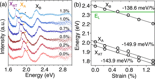
Figure 4. Differential-reflectance tracking of exciton energies under biaxial strain. (a) Normalized ΔR/R spectra showing the systematic red shift of the A and B excitons with increasing tensile biaxial strain. Purple and orange arrows indicate the A trion (XAT) and exciton (XA) positions, respectively. The background signal was subtracted from each spectrum for clarity. (b) Strain dependence of the XA, XB, and XAT energies. Linear fits yield a slope of −138.6 ± 10 meV/% for the B exciton, corresponding to a total shift of ∼−180 meV at ε = 1.3%. The green line marks the laser excitation energy (EL).
Figure 5
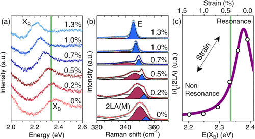
Figure 5. Strain-controlled transition between resonant and nonresonant 2LA(M) scattering. (a) B-exciton energy as a function of biaxial strain extracted from differential reflectance. The green horizontal line indicates the fixed laser excitation energy (2.33 eV). (b) Strain dependence of the E and 2LA(M) Raman modes positions. (c) Normalized intensity of the 2LA(M) as a function of B-exciton energy, showing a continuous suppression as the exciton is shifted away from resonance with the laser (green line). The upper horizontal axis indicates the corresponding biaxial strain. The purple solid line represents the effective resonance model used to quantify the detuning-dependent decay of the 2LA(M) intensity.
References
This article references 52 other publications.
- 1Niehues, I.; Schmidt, R.; Drüppel, M.; Marauhn, P.; Christiansen, D.; Selig, M.; Berghäuser, G.; Wigger, D.; Schneider, R.; Braasch, L.; Koch, R.; Castellanos-Gomez, A.; Kuhn, T.; Knorr, A.; Malic, E.; Rohlfing, M.; Michaelis de Vasconcellos, S.; Bratschitsch, R. Strain Control of Exciton-Phonon Coupling in Atomically Thin Semiconductors. Nano Lett. 2018, 18 (3), 1751– 1757, DOI: 10.1021/acs.nanolett.7b04868There is no corresponding record for this reference.
- 2Wang, G.; Chernikov, A.; Glazov, M. M.; Heinz, T. F.; Marie, X.; Amand, T.; Urbaszek, B. Colloquium: Excitons in Atomically Thin Transition Metal Dichalcogenides. Rev. Mod. Phys. 2018, 90 (2), 021001, DOI: 10.1103/RevModPhys.90.021001There is no corresponding record for this reference.
- 3Brem, S.; Ekman, A.; Christiansen, D.; Katsch, F.; Selig, M.; Robert, C.; Marie, X.; Urbaszek, B.; Knorr, A.; Malic, E. Phonon-Assisted Photoluminescence from Indirect Excitons in Monolayers of Transition-Metal Dichalcogenides. Nano Lett. 2020, 20 (4), 2849– 2856, DOI: 10.1021/acs.nanolett.0c00633There is no corresponding record for this reference.
- 4Dadgar, A. M.; Scullion, D.; Kang, K.; Esposito, D.; Yang, E. H.; Herman, I. P.; Pimenta, M. A.; Santos, E.-J. G.; Pasupathy, A. N. Strain Engineering and Raman Spectroscopy of Monolayer Transition Metal Dichalcogenides. Chem. Mater. 2018, 30 (15), 5148– 5155, DOI: 10.1021/acs.chemmater.8b01672There is no corresponding record for this reference.
- 5Peng, Z.; Chen, X.; Fan, Y.; Srolovitz, D. J.; Lei, D. Strain Engineering of 2D Semiconductors and Graphene: From Strain Fields to Band-Structure Tuning and Photonic Applications. Light: Sci. Appl. 2020, 9 (1), 190, DOI: 10.1038/s41377-020-00421-5There is no corresponding record for this reference.
- 6Hernández López, P.; Heeg, S.; Schattauer, C.; Kovalchuk, S.; Kumar, A.; Bock, D. J.; Kirchhof, J. N.; Höfer, B.; Greben, K.; Yagodkin, D.; Linhart, L.; Libisch, F.; Bolotin, K. I. Strain Control of Hybridization between Dark and Localized Excitons in a 2D Semiconductor. Nat. Commun. 2022, 13 (1), 7691, DOI: 10.1038/s41467-022-35352-9There is no corresponding record for this reference.
- 7Kumar, A. M.; Yagodkin, D.; Rosati, R.; Bock, D. J.; Schattauer, C.; Tobisch, S.; Hagel, J.; Höfer, B.; Kirchhof, J. N.; Hernández López, P.; Burfeindt, K.; Heeg, S.; Gahl, C.; Libisch, F.; Malic, E.; Bolotin, K. I. Strain Fingerprinting of Exciton Valley Character in 2D Semiconductors. Nat. Commun. 2024, 15 (1), 7546, DOI: 10.1038/s41467-024-51195-yThere is no corresponding record for this reference.
- 8Ronco, G.; Martínez-Suárez, A.; Tedeschi, D.; Savaresi, M.; Hierro-Rodríguez, A.; McVitie, S.; Stroj, S.; Aberl, J.; Brehm, M.; García-Suárez, V. M.; Rota, M. B.; Alonso-González, P.; Martín-Sánchez, J.; Trotta, R. Strain-Induced Exciton Redistribution among Quantum Emitters in Two-Dimensional Materials. npj 2D Mater. Appl. 2025, 9 (1), 65, DOI: 10.1038/s41699-025-00588-8There is no corresponding record for this reference.
- 9Negi, D.; Baishya, M.; Moghe, A. R.; Paul, S.; Badola, S.; Saha, S. Uniaxial Strain-Dependent Resonant Raman Scattering in WS2. Small 2025, 21 (17), 2412832, DOI: 10.1002/smll.202412832There is no corresponding record for this reference.
- 10Carrascoso, F.; Frisenda, R.; Castellanos-Gomez, A. Biaxial versus Uniaxial Strain Tuning of Single-Layer MoS2. Nano Mater. Sci. 2022, 4 (1), 44– 51, DOI: 10.1016/j.nanoms.2021.03.001There is no corresponding record for this reference.
- 11Kourmoulakis, G.; Michail, A.; Paradisanos, I.; Marie, X.; Glazov, M. M.; Jorissen, B.; Covaci, L.; Stratakis, E.; Papagelis, K.; Parthenios, J.; Kioseoglou, G. Biaxial Strain Tuning of Exciton Energy and Polarization in Monolayer WS2. Appl. Phys. Lett. 2023, 123 (22), 223103, DOI: 10.1063/5.0167724There is no corresponding record for this reference.
- 12Michail, A.; Anestopoulos, D.; Delikoukos, N.; Grammatikopoulos, S.; Tsirkas, S. A.; Lathiotakis, N. N.; Frank, O.; Filintoglou, K.; Parthenios, J.; Papagelis, K. Tuning the Photoluminescence and Raman Response of Single-Layer WS2 Crystals Using Biaxial Strain. J. Phys. Chem. C 2023, 127 (7), 3506– 3515, DOI: 10.1021/acs.jpcc.2c06933There is no corresponding record for this reference.
- 13Yang, J. A.; Bennett, R. K. A.; Hoang, L.; Zhang, Z.; Thompson, K. J.; Michail, A.; Parthenios, J.; Papagelis, K.; Mannix, A. J.; Pop, E. Biaxial Tensile Strain Enhances Electron Mobility of Monolayer Transition Metal Dichalcogenides. ACS Nano 2024, 18 (28), 18151– 18159, DOI: 10.1021/acsnano.3c08996There is no corresponding record for this reference.
- 14Oliva, R.; Wozniak, T.; Faria, P. E. J.; Dybala, F.; Kopaczek, J.; Fabian, J.; Scharoch, P.; Kudrawiec, R. Strong Substrate Strain Effects in Multilayered WS2 Revealed by High-Pressure Optical Measurements. ACS Appl. Mater. Interfaces 2022, 14 (17), 19857– 19868, DOI: 10.1021/acsami.2c01726There is no corresponding record for this reference.
- 15Gastaldo, M.; Varillas, J.; Rodríguez, Á.; Velický, M.; Frank, O.; Kalbáč, M. Tunable Strain and Bandgap in Subcritical-Sized MoS2 Nanobubbles. npj 2D Mater. Appl. 2023, 7 (1), 71, DOI: 10.1038/s41699-023-00432-xThere is no corresponding record for this reference.
- 16Henríquez-Guerra, E.; Li, H.; Pasqués-Gramage, P.; Gosálbez-Martínez, D.; D’Agosta, R.; Castellanos-Gomez, A.; Calvo, M. R. Large Biaxial Compressive Strain Tuning of Neutral and Charged Excitons in Single-Layer Transition Metal Dichalcogenides. ACS Appl. Mater. Interfaces 2023, 15 (49), 57369– 57378, DOI: 10.1021/acsami.3c13281There is no corresponding record for this reference.
- 17Manzanares-Negro, Y.; Zambudio, A.; López-Polín, G.; Sarkar, S.; Chhowalla, M.; Gómez-Herrero, J.; Gómez-Navarro, C. Fatigue Response of MoS2 with Controlled Introduction of Atomic Vacancies. Nano Lett. 2023, 23 (23), 10731– 10738, DOI: 10.1021/acs.nanolett.3c02479There is no corresponding record for this reference.
- 18Stellino, E.; D’Alò, B.; Blundo, E.; Postorino, P.; Polimeni, A. Fine-Tuning of the Excitonic Response in Monolayer WS2 Domes via Coupled Pressure and Strain Variation. Nano Lett. 2024, 24 (13), 3945– 3951, DOI: 10.1021/acs.nanolett.4c00157There is no corresponding record for this reference.
- 19Polimeno, L.; Di Renzo, A.; Manoccio, M. C.; Mastria, R.; De Giorgi, M.; Esposito, M.; Rizzo, A.; De Marco, L.; Ballarini, D.; Tasco, V.; Dominici, L.; Sanvitto, D.; Todisco, F. Energy Control of Strain-Induced Localized States in a WS2 Monolayer. Opt. Express 2025, 33 (25), 53165– 53172, DOI: 10.1364/OE.563119There is no corresponding record for this reference.
- 20Marchiani, D.; Jimenez-Arevalo, N.; Rago, I.; Pandolfi, F.; Cavoto, G.; Sbroscia, M.; Dudin, P.; Avila, J.; Mariani, C.; Betti, M. G.; Frisenda, R. Tensile Strain-Induced Bandgap Reduction and Exciton Recombination in a Trilayer MoS2 Nanosheet Wrinkle: Implications for Nanoscale Optoelectronic and Photonic Devices. ACS Appl. Nano Mater. 2025, 8 (42), 20230– 20238, DOI: 10.1021/acsanm.5c02997There is no corresponding record for this reference.
- 21Harats, M. G.; Kirchhof, J. N.; Qiao, M.; Greben, K.; Bolotin, K. I. Dynamics and Efficient Conversion of Excitons to Trions in Non-Uniformly Strained Monolayer WS2. Nat. Photonics 2020, 14 (5), 324– 329, DOI: 10.1038/s41566-019-0581-5There is no corresponding record for this reference.
- 22Rodriguez, A.; Kalbáč, M.; Frank, O. Strong Localization Effects in the Photoluminescence of Transition Metal Dichalcogenide Heterobilayers. 2D Mater. 2021, 8 (2), 025028, DOI: 10.1088/2053-1583/abe363There is no corresponding record for this reference.
- 23Roy, S.; Yang, X.; Gao, J. Biaxial Strain Tuned Upconversion Photoluminescence of Monolayer WS2. Sci. Rep. 2024, 14 (1), 3860, DOI: 10.1038/s41598-024-54185-8There is no corresponding record for this reference.
- 24Waheed, Y.; Shit, S.; Surendran, J. T.; Prasad, I. D.; Watanabe, K.; Taniguchi, T.; Kumar, S. Large Trion Binding Energy in Monolayer WS2 via Strain-Enhanced Electron-Phonon Coupling. Commun. Mater. 2025, 6 (1), 86, DOI: 10.1038/s43246-025-00809-zThere is no corresponding record for this reference.
- 25Rodríguez, Á.; Çakıroğlu, O.; Li, H.; Carrascoso, F.; Mompean, F.; Garcia-Hernandez, M.; Munuera, C.; Castellanos-Gomez, A. Improved Strain Transfer Efficiency in Large-Area Two-Dimensional MoS2 Obtained by Gold-Assisted Exfoliation. J. Phys. Chem. Lett. 2024, 15 (24), 6355– 6362, DOI: 10.1021/acs.jpclett.4c00855There is no corresponding record for this reference.
- 26Androulidakis, C.; Koukaras, E. N.; Parthenios, J.; Kalosakas, G.; Papagelis, K.; Galiotis, C. Graphene Flakes under Controlled Biaxial Deformation. Sci. Rep. 2016, 5 (1), 18219, DOI: 10.1038/srep18219There is no corresponding record for this reference.
- 27Michail, A.; Anestopoulos, D.; Delikoukos, N.; Parthenios, J.; Grammatikopoulos, S.; Tsirkas, S. A.; Lathiotakis, N. N.; Frank, O.; Filintoglou, K.; Papagelis, K. Biaxial Strain Engineering of CVD and Exfoliated Single- and Bi-Layer MoS2 Crystals. 2D Mater. 2021, 8 (1), 015023, DOI: 10.1088/2053-1583/abc2deThere is no corresponding record for this reference.
- 28Magda, G. Z.; Pető, J.; Dobrik, G.; Hwang, C.; Biró, L. P.; Tapasztó, L. Exfoliation of Large-Area Transition Metal Chalcogenide Single Layers. Sci. Rep. 2015, 5 (1), 14714, DOI: 10.1038/srep14714There is no corresponding record for this reference.
- 29Velický, M.; Donnelly, G. E.; Hendren, W. R.; McFarland, S.; Scullion, D.; DeBenedetti, W. J. I.; Correa, G. C.; Han, Y.; Wain, A. J.; Hines, M. A.; Muller, D. A.; Novoselov, K. S.; Abruña, H. D.; Bowman, R. M.; Santos, E. J. G.; Huang, F. Mechanism of Gold-Assisted Exfoliation of Centimeter-Sized Transition-Metal Dichalcogenide Monolayers. ACS Nano 2018, 12 (10), 10463– 10472, DOI: 10.1021/acsnano.8b06101There is no corresponding record for this reference.
- 30Velický, M.; Rodriguez, A.; Bouša, M.; Krayev, A. V.; Vondráček, M.; Honolka, J.; Ahmadi, M.; Donnelly, G. E.; Huang, F.; Abruña, H. D.; Novoselov, K. S.; Frank, O. Strain and Charge Doping Fingerprints of the Strong Interaction between Monolayer MoS2 and Gold. J. Phys. Chem. Lett. 2020, 11 (15), 6112– 6118, DOI: 10.1021/acs.jpclett.0c01287There is no corresponding record for this reference.
- 31Rodriguez, A.; Velický, M.; Řáhová, J.; Zólyomi, V.; Koltai, J.; Kalbáč, M.; Frank, O. Activation of Raman Modes in Monolayer Transition Metal Dichalcogenides through Strong Interaction with Gold. Phys. Rev. B 2022, 105 (19), 195413, DOI: 10.1103/PhysRevB.105.195413There is no corresponding record for this reference.
- 32Zhao, W.; Ghorannevis, Z.; Amara, K. K.; Pang, J. R.; Toh, M.; Zhang, X.; Kloc, C.; Tan, P. H.; Eda, G. Lattice Dynamics in Mono- and Few-Layer Sheets of WS2 and WSe2. Nanoscale 2013, 5 (20), 9677– 9683, DOI: 10.1039/c3nr03052kThere is no corresponding record for this reference.
- 33del Corro, E.; Botello-Méndez, A.; Gillet, Y.; Elias, A. L.; Terrones, H.; Feng, S.; Fantini, C.; Rhodes, D.; Pradhan, N.; Balicas, L.; Gonze, X.; Charlier, J.-C.; Terrones, M.; Pimenta, M. A. Atypical Exciton-Phonon Interactions in WS2 and WSe2 Monolayers Revealed by Resonance Raman Spectroscopy. Nano Lett. 2016, 16 (4), 2363– 2368, DOI: 10.1021/acs.nanolett.5b05096There is no corresponding record for this reference.
- 34Molas, M. R.; Nogajewski, K.; Potemski, M.; Babiński, A. Raman Scattering Excitation Spectroscopy of Monolayer WS2. Sci. Rep. 2017, 7 (1), 5036, DOI: 10.1038/s41598-017-05367-0There is no corresponding record for this reference.
- 35Liu, H.-L.; Yang, T.; Tatsumi, Y.; Zhang, Y.; Dong, B.; Guo, H.; Zhang, Z.; Kumamoto, Y.; Li, M.-Y.; Li, L.-J.; Saito, R.; Kawata, S. Deep-Ultraviolet Raman Scattering Spectroscopy of Monolayer WS2. Sci. Rep. 2018, 8 (1), 11398, DOI: 10.1038/s41598-018-29587-0There is no corresponding record for this reference.
- 36Berkdemir, A.; Gutiérrez, H. R.; Botello-Méndez, A. R.; Perea-López, N.; Elías, A. L.; Chia, C.-I.; Wang, B.; Crespi, V. H.; López-Urías, F.; Charlier, J.-C.; Terrones, H.; Terrones, M. Identification of Individual and Few Layers of WS2 Using Raman Spectroscopy. Sci. Rep. 2013, 3 (1), 1755, DOI: 10.1038/srep01755There is no corresponding record for this reference.
- 37Chen, S.-Y.; Zheng, C.; Fuhrer, M. S.; Yan, J. Helicity-Resolved Raman Scattering of MoS2, MoSe2, WS2, and WSe2 Atomic Layers. Nano Lett. 2015, 15 (4), 2526– 2532, DOI: 10.1021/acs.nanolett.5b00092There is no corresponding record for this reference.
- 38Carvalho, B. R.; Wang, Y.; Mignuzzi, S.; Roy, D.; Terrones, M.; Fantini, C.; Crespi, V. H.; Malard, L. M.; Pimenta, M. A. Intervalley Scattering by Acoustic Phonons in Two-Dimensional MoS2 Revealed by Double-Resonance Raman Spectroscopy. Nat. Commun. 2017, 8 (1), 14670, DOI: 10.1038/ncomms14670There is no corresponding record for this reference.
- 39Mohiuddin, T. M. G.; Lombardo, A.; Nair, R. R.; Bonetti, A.; Savini, G.; Jalil, R.; Bonini, N.; Basko, D. M.; Galiotis, C.; Marzari, N.; Novoselov, K. S.; Geim, A. K.; Ferrari, A. C. Uniaxial Strain in Graphene by Raman Spectroscopy: $G$ Peak Splitting, Gr\″uneisen Parameters, and Sample Orientation. Phys. Rev. B 2009, 79 (20), 205433, DOI: 10.1103/PhysRevB.79.205433There is no corresponding record for this reference.
- 40del Corro, E.; de la Roza, A. O.; Taravillo, M.; Baonza, V. G. Raman Modes and Grüneisen Parameters of Graphite under Compressive Biaxial Stress. Carbon N. Y. 2012, 50 (12), 4600– 4606, DOI: 10.1016/j.carbon.2012.05.046There is no corresponding record for this reference.
- 41Chernikov, A.; Berkelbach, T. C.; Hill, H. M.; Rigosi, A.; Li, Y.; Aslan, B.; Reichman, D. R.; Hybertsen, M. S.; Heinz, T. F. Exciton Binding Energy and Nonhydrogenic Rydberg Series in Monolayer WS2. Phys. Rev. Lett. 2014, 113 (7), 76802, DOI: 10.1103/PhysRevLett.113.076802There is no corresponding record for this reference.
- 42Raja, A.; Chaves, A.; Yu, J.; Arefe, G.; Hill, H. M.; Rigosi, A. F.; Berkelbach, T. C.; Nagler, P.; Schüller, C.; Korn, T.; Nuckolls, C.; Hone, J.; Brus, L. E.; Heinz, T. F.; Reichman, D. R.; Chernikov, A. Coulomb Engineering of the Bandgap and Excitons in Two-Dimensional Materials. Nat. Commun. 2017, 8 (1), 15251, DOI: 10.1038/ncomms15251There is no corresponding record for this reference.
- 43Carrascoso, F.; Lin, D.-Y.; Frisenda, R.; Castellanos-Gomez, A. Biaxial Strain Tuning of Interlayer Excitons in Bilayer MoS2. J. Phys. Mater. 2020, 3 (1), 015003, DOI: 10.1088/2515-7639/ab4432There is no corresponding record for this reference.
- 44Frisenda, R.; Drüppel, M.; Schmidt, R.; Michaelis de Vasconcellos, S.; Perez de Lara, D.; Bratschitsch, R.; Rohlfing, M.; Castellanos-Gomez, A. Biaxial Strain Tuning of the Optical Properties of Single-Layer Transition Metal Dichalcogenides. npj 2D Mater. Appl. 2017, 1 (1), 10, DOI: 10.1038/s41699-017-0013-7There is no corresponding record for this reference.
- 45Zollner, K.; Junior, P. E. F.; Fabian, J. Strain-Tunable Orbital, Spin-Orbit, and Optical Properties of Monolayer Transition-Metal Dichalcogenides. Phys. Rev. B 2019, 100 (19), 195126, DOI: 10.1103/PhysRevB.100.195126There is no corresponding record for this reference.
- 46He, K.; Poole, C.; Mak, K. F.; Shan, J. Experimental Demonstration of Continuous Electronic Structure Tuning via Strain in Atomically Thin MoS2. Nano Lett. 2013, 13 (6), 2931– 2936, DOI: 10.1021/nl4013166There is no corresponding record for this reference.
- 47Conley, H. J.; Wang, B.; Ziegler, J. I.; Haglund, R. F. J.; Pantelides, S. T.; Bolotin, K. I. Bandgap Engineering of Strained Monolayer and Bilayer MoS2. Nano Lett. 2013, 13 (8), 3626– 3630, DOI: 10.1021/nl4014748There is no corresponding record for this reference.
- 48Castellanos-Gomez, A.; Roldán, R.; Cappelluti, E.; Buscema, M.; Guinea, F.; van der Zant, H. S. J.; Steele, G. A. Local Strain Engineering in Atomically Thin MoS2. Nano Lett. 2013, 13 (11), 5361– 5366, DOI: 10.1021/nl402875mThere is no corresponding record for this reference.
- 49Lemos, J. S.; Blundo, E.; Polimeni, A.; Pimenta, M. A.; Righi, A. Exciton-Phonon Interactions in Strained Domes of Monolayer MoS2 Studied by Resonance Raman Spectroscopy. Nanomaterials. 2023, 13, 2722, DOI: 10.3390/nano13192722There is no corresponding record for this reference.
- 50Soubelet, P.; Bruchhausen, A. E.; Fainstein, A.; Nogajewski, K.; Faugeras, C. Resonance Effects in the Raman Scattering of Monolayer and Few-Layer MoSe2. Phys. Rev. B 2016, 93 (15), 155407, DOI: 10.1103/PhysRevB.93.155407There is no corresponding record for this reference.
- 51Shi, L.; Rohringer, P.; Wanko, M.; Rubio, A.; Waßerroth, S.; Reich, S.; Cambré, S.; Wenseleers, W.; Ayala, P.; Pichler, T. Electronic Band Gaps of Confined Linear Carbon Chains Ranging from Polyyne to Carbyne. Phys. Rev. Mater. 2017, 1 (7), 075601, DOI: 10.1103/PhysRevMaterials.1.075601There is no corresponding record for this reference.
- 52Heeg, S.; Shi, L.; Pichler, T.; Novotny, L. Raman Resonance Profile of an Individual Confined Long Linear Carbon Chain. Carbon N. Y. 2018, 139, 581– 585, DOI: 10.1016/j.carbon.2018.07.007There is no corresponding record for this reference.
Supporting Information
Supporting Information
The Supporting Information is available free of charge at https://pubs.acs.org/doi/10.1021/acsphotonics.5c03089.
Experimental methods, images of the experimental biaxial setup, AFM images of the samples, spatial uniformity of the applied biaxial strain, additional Raman datasets for monolayer and bilayer WS2, raw data of differential reflectance spectra, experiments demonstrating the reversibility of the applied strain under biaxial strain, and details of the theoretical detuning model (PDF)
Terms & Conditions
Most electronic Supporting Information files are available without a subscription to ACS Web Editions. Such files may be downloaded by article for research use (if there is a public use license linked to the relevant article, that license may permit other uses). Permission may be obtained from ACS for other uses through requests via the RightsLink permission system: http://pubs.acs.org/page/copyright/permissions.html.