


This publication is free to access through this site. Learn More

ACS Editors' Choice® is a collection designed to feature scientific articles of broad public interest. Read the latest articles
Optical Engineering of Colloidal Quantum Dot Films: From Effective-Medium to Device ArchitecturesClick to copy article linkArticle link copied!
- Jugyoung KimJugyoung KimDepartment of Energy Science, Sungkyunkwan University, Suwon 16419, Republic of KoreaMore by Jugyoung Kim
- Ha-Chi V. TranHa-Chi V. TranDepartment of Energy Science, Sungkyunkwan University, Suwon 16419, Republic of KoreaMore by Ha-Chi V. Tran
- Sohee Jeong*Sohee Jeong*Email: [email protected]Department of Energy Science, Sungkyunkwan University, Suwon 16419, Republic of KoreaDepartment of Future Energy Engineering, Sungkyunkwan University, Suwon 16419, Republic of KoreaSungkyunkwan Institute of Energy Science and Technology, Suwon 16419, Republic of KoreaMore by Sohee Jeong
Abstract
Colloidal quantum dots (CQDs) are promising candidates for next-generation infrared optoelectronics. While maximizing external quantum efficiency─a key figure of merit for photodetectors and photovoltaics─requires both enhanced light absorption and efficient carrier extraction, the former has received comparatively less attention. This work presents a framework for tailoring the optical properties of CQD films to engineer enhanced absorption in optoelectronic devices. Using effective-medium theory, we discuss how the complex refractive index of CQD films can be modeled and how their optical constants can be systematically related to the quantum dot size, ligand length, and shape. Employing transfer-matrix method calculations, we show how to optimize multilayer stacks by utilizing Fabry–Pérot resonances to maximize absorption. We also present methods to mitigate parasitic losses that limit the absorptance. This framework helps to diagnose whether the device performance is limited by absorption or by carrier extraction and guides research directions toward overcoming these limits. Finally, we discuss the limitations of current theoretical models and propose future directions for extending these principles to emerging optoelectronic applications.
This publication is licensed for personal use by The American Chemical Society.
Introduction
Modeling the Optical Response of CQD Thin Films: An EMT
Figure 1
Figure 1. Effective-medium view of CQD films. Top: A heterogeneous CQD film comprises inorganic CQD cores, organic ligands, and interparticle voids; microstructural attributes─core size/shape and interdot spacing─govern packing. Bottom: In EMT, the film is replaced by a homogeneous medium with complex permittivity (ε̃eff); the CQD cores (ε̃core) act as inclusions embedded in a host of ligands and voids (ε̃h). The volume fractions fcore and fh encode the microstructure; the panels on the right illustrate different volume fractions.
Experimental Determination of the Effective Optical Constants in CQD Thin Films
Effective-Medium Perspective on CQD Film Optical Constants
Figure 2
Figure 2. Complex refractive index of the CdSe cores and CdSe/CdS core–shell nanocrystals extracted in solution (a) and thin films (b). Adapted with permission from ref (35). Copyright 2018 American Chemical Society. The average refractive index of PbS CQD films from ellipsometry (symbols) and fNC (blue), obtained by fitting the ellipsometry data using the Bruggeman model or by a hard-sphere model (orange), plotted as a function of the PbS CQD excitonic peak (c) and surface ligand (d). Adapted with permission from ref (38). Copyright 2022 Royal Society of Chemistry. Real part of the effective dielectric function (e) and transfer curve (f) for InAs CQD films composed of tetrahedra (red) or spheres (blue) with identical particle volume (32 nm3). Adapted from ref (42) under the CC BY-NC-ND license. Copyright 2024 American Chemical Society.
Optical-Cavity Engineering in CQD Photodiodes for IR Optoelectronics
Figure 3
Figure 3. (a) Multilayer CQD photodiode (TCO/ETL/CQD absorber/HTL/metal) forming a FP cavity. (b) TMM: each layer with thickness di and complex index Ñi represented by Mi. The total transfer matrix (M) relates to the incident and reflected fields. (c) Simulated electric-field intensity (|E| 2) vs wavelength (1100–1600 nm) and position. A resonance near 1.3 μm concentrates the field in the CQD layer. (d) Calculated nanocrystal absorption vs CQD film thickness and wavelength. Slanted bands are FP resonances. Adapted with permission from ref (38). Copyright 2022 Royal Society of Chemistry.
Optimizing the Thickness of the CQD Absorbing Layer for Enhanced Device Performance
Figure 4
Figure 4. Thickness optimization of CQD absorbers. (a) PbS SWIR PD: TMM absorptance at the excitonic peak vs active-layer thickness (black) with measured EQE at 1550 nm under −2 V (red). Data from ref (47). (b) Micrometer-thick PbS CQD solar cell: EQE (purple) with the AM1.5G spectrum (gray). Adapted with permission from ref (50). Copyright 2020 American Chemical Society. (c) InAs NIR PD: TMM absorptance vs film thickness with representative reported EQEs (colored symbols). (d) Expected EQE from TMM (black) vs measured EQE (red circles) at 940 nm. (e) Thickness and bias dependent EQE (f) Specific detectivity at −1 V vs thickness (inset, EQE spectra). Adapted with permission from ref (51). Copyright 2024 Wiley-VCH GMbH.
Optical-Spacer Engineering for Enhanced CQD Photodiode Performance
Figure 5
Figure 5. Optical-spacer engineering in CQD photodiodes. PbS SWIR PD with a MoOx IBL: (a) Simulated absorptance vs active-layer thickness for MoOx = 0, 10, 25, and 40 nm. (b) Specific detectivity at −1 V and dark current–voltage characteristics (inset) for devices with MoOx (black) and without MoOx (blue). Adapted with permission from ref (47). Copyright 2025 American Chemical Society. InAs CQD IR solar cell with a p-type optical spacer: (c) Simulated EQE vs p-InAs thickness for n-type absorber thicknesses of 90, 110, and 120 nm. 2D electric-field-intensity maps without (d) and with a 30 nm p-InAs layer (e). (f) Measured EQE (solid) for p-InAs thickness = 0, 15, and 30 nm and calculated integrated Jsc. Adapted with permission from ref (52). Copyright 2024 Wiley-VCH GMbH.
Minimizing Parasitic Absorption through Advanced Electrode Engineering
Figure 6
Figure 6. Advanced electrode designs for IR CQD solar cells. DBR cavity: (a) Schematic of reflective top contact and a DBR mirror contact, forming an optical cavity that enhances IR multipass. (b) EQE of the cavity device (red) versus a control without the cavity (black), showing enhancement near 1.3 μm. Adapted with permission from ref (53). Copyright 2016 American Chemical Society. Transparent IMZ electrode: (c) Transmittance of the IMZ asymmetric multilayer (red) compared with ITO (black dashed) over 1000–1800 nm at comparable sheet resistance (≈10 Ω sq–1); inset: IMZ stack. (d) EQE with ITO (black dashed), IMZ without Ag (yellow), and IMZ (red), demonstrating performance gains from the multilayer electrode. Adapted with permission from ref (54). Copyright 2018 American Chemical Society.
Conclusion and Outlook
Challenges and Opportunities in CQD Optical Characterization
Expanding CQD Applications through Advanced Photonic Architecture
Author Information
- Sohee Jeong - Department of Energy Science, Sungkyunkwan University, Suwon 16419, Republic of Korea; Department of Future Energy Engineering, Sungkyunkwan University, Suwon 16419, Republic of Korea; Sungkyunkwan Institute of Energy Science and Technology, Suwon 16419, Republic of Korea;
 https://orcid.org/0000-0002-9863-1374;
The manuscript was written through contributions of all authors. All authors have given approval to the final version of the manuscript.
This research was supported by the National Research Foundation, funded by the Ministry of Science and ICT (RS-2022-NR070449 and RS-2024-00444458). It was also supported by Grants RS-2022-00144108 and RS-2024-00418086, funded by the Ministry of Trade, Industry, and Energy of the Korean Government.
References
This article references 80 other publications.
- 1Karani, A.; Yang, L.; Bai, S.; Futscher, M. H.; Snaith, H. J.; Ehrler, B.; Greenham, N. C.; Di, D. Perovskite/colloidal quantum dot tandem solar cells: theoretical modeling and monolithic structure. ACS Energy Lett. 2018, 3 (4), 869– 874, DOI: 10.1021/acsenergylett.8b00207Google ScholarThere is no corresponding record for this reference.
- 2Semonin, O. E.; Luther, J. M.; Beard, M. C. Quantum dots for next-generation photovoltaics. Mater. Today 2012, 15 (11), 508– 515, DOI: 10.1016/S1369-7021(12)70220-1Google ScholarThere is no corresponding record for this reference.
- 3Cao, F.; Liu, L.; Li, L. Short-wave infrared photodetector. Mater. Today 2023, 62, 327– 349, DOI: 10.1016/j.mattod.2022.11.003Google ScholarThere is no corresponding record for this reference.
- 4Wiley, L.; Cavanaugh, R.; Follansbee, J.; Burrell, D.; Grimming, R.; Pimpinella, R.; Voss, J.; Furxhi, O.; Driggers, R. Comparison of reflective band (Vis, NIR, SWIR, eSWIR) performance in daytime reduced illumination conditions. Appl. Opt. 2023, 62 (31), 8316– 8326, DOI: 10.1364/AO.495832Google ScholarThere is no corresponding record for this reference.
- 5Polman, A.; Knight, M.; Garnett, E. C.; Ehrler, B.; Sinke, W. C. Photovoltaic materials: Present efficiencies and future challenges. Science 2016, 352 (6283), aad4424, DOI: 10.1126/science.aad4424Google ScholarThere is no corresponding record for this reference.
- 6Sargent, E. H. Solar cells, photodetectors, and optical sources from infrared colloidal quantum dots. Adv. Mater. 2008, 20 (20), 3958– 3964, DOI: 10.1002/adma.200801153Google ScholarThere is no corresponding record for this reference.
- 7García de Arquer, F. P.; Talapin, D. V.; Klimov, V. I.; Arakawa, Y.; Bayer, M.; Sargent, E. H. Semiconductor quantum dots: Technological progress and future challenges. Science 2021, 373 (6555), eaaz8541 DOI: 10.1126/science.aaz8541Google ScholarThere is no corresponding record for this reference.
- 8Kim, M.; Choi, M.; Choi, S.; Jeong, S. Semiconductor nanocrystals: Unveiling the chemistry behind different facets. Acc. Chem. Res. 2023, 56 (13), 1756– 1765, DOI: 10.1021/acs.accounts.3c00123Google ScholarThere is no corresponding record for this reference.
- 9Pinna, J.; Mehrabi Koushki, R.; Gavhane, D. S.; Ahmadi, M.; Mutalik, S.; Zohaib, M.; Protesescu, L.; Kooi, B. J.; Portale, G.; Loi, M. A. Approaching bulk mobility in PbSe colloidal quantum dots 3D superlattices. Adv. Mater. 2023, 35 (8), 2207364, DOI: 10.1002/adma.202207364Google ScholarThere is no corresponding record for this reference.
- 10Kagan, C. R.; Murray, C. B. Charge transport in strongly coupled quantum dot solids. Nat. Nanotechnol. 2015, 10 (12), 1013– 1026, DOI: 10.1038/nnano.2015.247Google ScholarThere is no corresponding record for this reference.
- 11Liu, Y.; Gibbs, M.; Puthussery, J.; Gaik, S.; Ihly, R.; Hillhouse, H. W.; Law, M. Dependence of carrier mobility on nanocrystal size and ligand length in PbSe nanocrystal solids. Nano Lett. 2010, 10 (5), 1960– 1969, DOI: 10.1021/nl101284kGoogle ScholarThere is no corresponding record for this reference.
- 12Bederak, D.; Balazs, D. M.; Sukharevska, N. V.; Shulga, A. G.; Abdu-Aguye, M.; Dirin, D. N.; Kovalenko, M. V.; Loi, M. A. Comparing halide ligands in PbS colloidal quantum dots for field-effect transistors and solar cells. ACS Appl. Nano Mater. 2018, 1 (12), 6882– 6889, DOI: 10.1021/acsanm.8b01696Google ScholarThere is no corresponding record for this reference.
- 13Septianto, R. D.; Miranti, R.; Kikitsu, T.; Hikima, T.; Hashizume, D.; Matsushita, N.; Iwasa, Y.; Bisri, S. Z. Enabling metallic behaviour in two-dimensional superlattice of semiconductor colloidal quantum dots. Nat. Commun. 2023, 14, 2670, DOI: 10.1038/s41467-023-38216-yGoogle ScholarThere is no corresponding record for this reference.
- 14Choi, M.; Kim, M.; Lee, Y.; Kim, T.; Kim, J. H.; Shin, D.; Kim, J. W.; Kim, Y. H.; Jeong, S. Tailored band edge positions by fractional ligand replacement of nonconductive colloidal quantum dot films. J. Phys. Chem. C 2023, 127 (9), 4825– 4832, DOI: 10.1021/acs.jpcc.3c00376Google ScholarThere is no corresponding record for this reference.
- 15Kroupa, D. M.; Vörös, M.; Brawand, N. P.; McNichols, B. W.; Miller, E. M.; Gu, J.; Nozik, A. J.; Sellinger, A.; Galli, G.; Beard, M. C. Tuning colloidal quantum dot band edge positions through solution-phase surface chemistry modification. Nat. Commun. 2017, 8, 15257, DOI: 10.1038/ncomms15257Google ScholarThere is no corresponding record for this reference.
- 16Song, J. H.; Choi, H.; Pham, H. T.; Jeong, S. Energy level tuned indium arsenide colloidal quantum dot films for efficient photovoltaics. Nat. Commun. 2018, 9, 4267, DOI: 10.1038/s41467-018-06399-4Google ScholarThere is no corresponding record for this reference.
- 17Brown, P. R.; Kim, D.; Lunt, R. R.; Zhao, N.; Bawendi, M. G.; Grossman, J. C.; Bulović, V. Energy level modification in lead sulfide quantum dot thin films through ligand exchange. ACS Nano 2014, 8 (6), 5863– 5872, DOI: 10.1021/nn500897cGoogle ScholarThere is no corresponding record for this reference.
- 18Chehaibou, B.; Reiss, P.; Lhuillier, E.; Mugny, G.; Delerue, C.; Arnaud, A. Colloidal quantum dots thin films: A theoretical insight into optical efficiency for optoelectronic applications. IEEE Trans. Electron Devices 2025, 72 (2), 712– 722, DOI: 10.1109/TED.2024.3517595Google ScholarThere is no corresponding record for this reference.
- 19Nayak, J. K.; Chaudhuri, P. R.; Ratha, S.; Sahoo, M. R. A comprehensive review on effective medium theories to find effective dielectric constant of composites. J. Electromagn. Waves Appl. 2023, 37 (2), 282– 322, DOI: 10.1080/09205071.2022.2135029Google ScholarThere is no corresponding record for this reference.
- 20Konstantatos, G.; Sargent, E. H. Colloidal quantum dot photodetectors. Infrared Phys. Technol. 2011, 54 (3), 278– 282, DOI: 10.1016/j.infrared.2010.12.029Google ScholarThere is no corresponding record for this reference.
- 21Lin, W. M. M.; Yazdani, N.; Yarema, O.; Yarema, M.; Liu, M.; Sargent, E. H.; Kirchartz, T.; Wood, V. Recombination dynamics in PbS nanocrystal quantum dot solar cells studied through drift–diffusion simulations. ACS Appl. Electron. Mater. 2021, 3 (11), 4977– 4989, DOI: 10.1021/acsaelm.1c00787Google ScholarThere is no corresponding record for this reference.
- 22Clifford, J. P.; Konstantatos, G.; Johnston, K. W.; Hoogland, S.; Levina, L.; Sargent, E. H. Fast, sensitive and spectrally tuneable colloidal-quantum-dot photodetectors. Nat. Nanotechnol. 2009, 4 (1), 40– 44, DOI: 10.1038/nnano.2008.313Google ScholarThere is no corresponding record for this reference.
- 23Chuang, C. H. M.; Brown, P. R.; Bulović, V.; Bawendi, M. G. Improved performance and stability in quantum dot solar cells through band alignment engineering. Nat. Mater. 2014, 13 (8), 796– 801, DOI: 10.1038/nmat3984Google ScholarThere is no corresponding record for this reference.
- 24Zhitomirsky, D.; Voznyy, O.; Levina, L.; Hoogland, S.; Kemp, K. W.; Ip, A. H.; Thon, S. M.; Sargent, E. H. Engineering colloidal quantum dot solids within and beyond the mobility-invariant regime. Nat. Commun. 2014, 5, 3803, DOI: 10.1038/ncomms4803Google ScholarThere is no corresponding record for this reference.
- 25Lim, C.; Choi, M.; Kim, T.; Shin, D.; Song, J. H.; Jeong, S. Effect of bandgap variation on photovoltaic properties of lead sulfide quantum dot solar cell. Mater. Today Energy 2023, 36, 101357, DOI: 10.1016/j.mtener.2023.101357Google ScholarThere is no corresponding record for this reference.
- 26Li, M.; Yan, J.; Zhao, X.; Ma, T.; Zhang, A.; Chen, S.; Shen, G.; Khalaf, G. M. G.; Zhang, J.; Chen, C.; Hsu, H. Y.; Song, H.; Yang, P.; Tang, J. Synergistic enhancement of efficient perovskite/quantum dot tandem solar cells based on transparent electrode and band alignment engineering. Adv. Energy Mater. 2024, 14 (23), 2400219, DOI: 10.1002/aenm.202400219Google ScholarThere is no corresponding record for this reference.
- 27Valiei, M.; Shaibani, P. M.; Abdizadeh, H.; Kolahdouz, M.; Asl Soleimani, E.; Poursafar, J. Design and optimization of single, double and multilayer anti-reflection coatings on planar and textured surface of silicon solar cells. Mater. Today Commun. 2022, 32, 104144, DOI: 10.1016/j.mtcomm.2022.104144Google ScholarThere is no corresponding record for this reference.
- 28Beyer, B.; Leo, K. Efficiency increase of organic solar cells with emissive light-in-coupling layers. J. Mater. Chem. C 2015, 3 (41), 10830– 10836, DOI: 10.1039/C5TC02446CGoogle ScholarThere is no corresponding record for this reference.
- 29Kholmicheva, N.; Moroz, P.; Rijal, U.; Bastola, E.; Uprety, P.; Liyanage, G.; Razgoniaev, A.; Ostrowski, A. D.; Zamkov, M. Plasmonic nanocrystal solar cells utilizing strongly confined radiation. ACS Nano 2014, 8 (12), 12549– 12559, DOI: 10.1021/nn505375nGoogle ScholarThere is no corresponding record for this reference.
- 30Hong, J.; Kim, B. S.; Hou, B.; Cho, Y.; Lee, S. H.; Pak, S.; Morris, S. M.; Sohn, J. I.; Cha, S. N. Plasmonic effects of dual-metal nanoparticle layers for high-performance quantum dot solar cells. Plasmonics 2020, 15 (4), 1007– 1013, DOI: 10.1007/s11468-020-01120-yGoogle ScholarThere is no corresponding record for this reference.
- 31Tabernig, S. W.; Yuan, L.; Cordaro, A.; Teh, Z. L.; Gao, Y.; Patterson, R. J.; Pusch, A.; Huang, S.; Polman, A. Optically resonant bulk heterojunction PbS quantum dot solar cell. ACS Nano 2022, 16 (9), 13750– 13760, DOI: 10.1021/acsnano.1c11330Google ScholarThere is no corresponding record for this reference.
- 32Labelle, A. J.; Thon, S. M.; Masala, S.; Adachi, M. M.; Dong, H.; Farahani, M.; Ip, A. H.; Fratalocchi, A.; Sargent, E. H. Colloidal quantum dot solar cells exploiting hierarchical structuring. Nano Lett. 2015, 15 (2), 1101– 1108, DOI: 10.1021/nl504086vGoogle ScholarThere is no corresponding record for this reference.
- 33Kim, T.; Jin, X.; Song, J. H.; Jeong, S.; Park, T. Efficiency limit of colloidal quantum dot solar cells: effect of optical interference on active layer absorption. ACS Energy Lett. 2020, 5 (1), 248– 251, DOI: 10.1021/acsenergylett.9b02504Google ScholarThere is no corresponding record for this reference.
- 34Markel, V. A. Introduction to the Maxwell Garnett approximation: tutorial. J. Opt. Soc. Am. A 2016, 33 (7), 1244– 1256, DOI: 10.1364/JOSAA.33.001244Google ScholarThere is no corresponding record for this reference.
- 35Dement, D. B.; Puri, M.; Ferry, V. E. Determining the complex refractive index of neat CdSe/CdS quantum dot films. J. Phys. Chem. C 2018, 122 (37), 21557– 21568, DOI: 10.1021/acs.jpcc.8b04522Google ScholarThere is no corresponding record for this reference.
- 36Grinolds, D. D. W.; Brown, P. R.; Harris, D. K.; Bulović, V.; Bawendi, M. G. Quantum-dot size and thin-film dielectric constant: precision measurement and disparity with simple models. Nano Lett. 2015, 15 (1), 21– 26, DOI: 10.1021/nl5024244Google ScholarThere is no corresponding record for this reference.
- 37Murray, C. B.; Kagan, C. R.; Bawendi, M. G. Synthesis and characterization of monodisperse nanocrystals and close-packed nanocrystal assemblies. Annu. Rev. Mater. Sci. 2000, 30 (1), 545– 610, DOI: 10.1146/annurev.matsci.30.1.545Google ScholarThere is no corresponding record for this reference.
- 38Chehaibou, B.; Izquierdo, E.; Chu, A.; Abadie, C.; Cavallo, M.; Khalili, A.; Dang, T. H.; Gréboval, C.; Xu, X. Z.; Ithurria, S.; Vincent, G.; Gallas, B.; Mugny, G.; Arnaud, A.; Lhuillier, E.; Delerue, C. The complex optical index of PbS nanocrystal thin films and their use for short wave infrared sensor design. Nanoscale 2022, 14 (7), 2711– 2721, DOI: 10.1039/D1NR07770HGoogle ScholarThere is no corresponding record for this reference.
- 39Diroll, B. T.; Gaulding, E. A.; Kagan, C. R.; Murray, C. B. Spectrally-resolved dielectric functions of solution-cast quantum dot thin films. Chem. Mater. 2015, 27 (18), 6463– 6469, DOI: 10.1021/acs.chemmater.5b02953Google ScholarThere is no corresponding record for this reference.
- 40Zhang, Z.; Thung, Y. T.; Chen, X.; Wang, L.; Fan, W.; Ding, L.; Sun, H. Study of complex optical constants of neat cadmium selenide nanoplatelets thin films by spectroscopic ellipsometry. J. Phys. Chem. Lett. 2021, 12 (1), 191– 198, DOI: 10.1021/acs.jpclett.0c03304Google ScholarThere is no corresponding record for this reference.
- 41Rastogi, P.; Chu, A.; Dang, T. H.; Prado, Y.; Gréboval, C.; Qu, J.; Dabard, C.; Khalili, A.; Dandeu, E.; Fix, B.; Xu, X. Z.; Ithurria, S.; Vincent, G.; Gallas, B.; Lhuillier, E. Complex optical index of HgTe nanocrystal infrared thin films and its use for short-wave infrared photodiode design. Adv. Opt. Mater. 2021, 9 (10), 2002066, DOI: 10.1002/adom.202002066Google ScholarThere is no corresponding record for this reference.
- 42Kim, M.; Lee, J.; Jung, J.; Shin, D.; Kim, J.; Cho, E.; Xing, Y.; Jeong, H.; Park, S.; Oh, S. H.; Kim, Y. H.; Jeong, S. Surface-originated weak confinement in tetrahedral indium arsenide quantum dots. J. Am. Chem. Soc. 2024, 146 (15), 10251– 10256, DOI: 10.1021/jacs.4c00966Google ScholarThere is no corresponding record for this reference.
- 43Pettersson, L. A. A.; Roman, L. S.; Inganäs, O. Modeling photocurrent action spectra of photovoltaic devices based on organic thin films. J. Appl. Phys. 1999, 86 (1), 487– 496, DOI: 10.1063/1.370757Google ScholarThere is no corresponding record for this reference.
- 44Burkhard, G. F.; Hoke, E. T.; McGehee, M. D. Accounting for interference, scattering, and electrode absorption to make accurate internal quantum efficiency measurements in organic and other thin solar cells. Adv. Mater. 2010, 22 (30), 3293– 3297, DOI: 10.1002/adma.201000883Google ScholarThere is no corresponding record for this reference.
- 45Luce, A.; Mahdavi, A.; Marquardt, F.; Wankerl, H. TMM-Fast, a transfer matrix computation package for multilayer thin-film optimization: tutorial. J. Opt. Soc. Am. A 2022, 39 (6), 1007– 1013, DOI: 10.1364/JOSAA.450928Google ScholarThere is no corresponding record for this reference.
- 46Ouellette, O.; Lesage-Landry, A.; Scheffel, B.; Hoogland, S.; García de Arquer, F. P.; Sargent, E. H. Spatial collection in colloidal quantum dot solar cells. Adv. Funct. Mater. 2020, 30 (1), 1908200, DOI: 10.1002/adfm.201908200Google ScholarThere is no corresponding record for this reference.
- 47Tran, H. C. V.; Jang, E.; Kim, J.; Choi, M.; Park, Y.; Jeong, H.; Goo, T.; Bae, S.; Jeong, S. Enhanced SWIR photodetection in colloidal quantum dot photodiodes via tunneling current suppression. ACS Appl. Mater. Interfaces 2025, 17 (10), 15666– 15674, DOI: 10.1021/acsami.4c22853Google ScholarThere is no corresponding record for this reference.
- 48Huang, Y.; Hao, L.; Shao, L.; Tan, Z.; Li, S.; Dong, S.; Yang, X.; Zhong, W.; Wang, Y.; Huang, F. Near-infrared organic photodetectors with tailored junction thickness for resonance-enhanced photoresponse and suppressed dark current. ACS Photonics 2025, 12 (7), 3928– 3938, DOI: 10.1021/acsphotonics.5c01055Google ScholarThere is no corresponding record for this reference.
- 49Ooi, Z. Y.; Nie, S.; Vega, G.; Lai, M. C.; Jiménez-Solano, A.; Huang, C. S.; Wang, H.; Liu, T.; Gałkowski, K.; Nowak, M. P.; Nyga, P.; Cheng, Q.; Ducati, C.; Carretero-Palacios, S.; Kahmann, S.; Stranks, S. D.; Anaya, M. Resonant cavity effect for spectrally tunable and efficient narrowband perovskite photodetectors. ACS Photonics 2025, 12 (8), 4119– 4129, DOI: 10.1021/acsphotonics.4c01942Google ScholarThere is no corresponding record for this reference.
- 50Fan, J. Z.; Vafaie, M.; Bertens, K.; Sytnyk, M.; Pina, J. M.; Sagar, L. K.; Ouellette, O.; Proppe, A. H.; Rasouli, A. S.; Gao, Y.; Baek, S. W.; Chen, B.; Laquai, F.; Hoogland, S.; De Arquer, F. P. G.; Heiss, W.; Sargent, E. H. Micron thick colloidal quantum dot solids. Nano Lett. 2020, 20 (7), 5284– 5291, DOI: 10.1021/acs.nanolett.0c01614Google ScholarThere is no corresponding record for this reference.
- 51Shin, D.; Jeong, H.; Kim, J.; Jang, E.; Park, Y.; Jeong, S. High-performance infrared InAs colloidal quantum dot photodetector with 79% EQE enabled by an extended absorber layer. Adv. Opt. Mater. 2025, 13 (1), 2401931, DOI: 10.1002/adom.202401931Google ScholarThere is no corresponding record for this reference.
- 52Park, Y.; Kim, J.; Jeong, M.; Shin, D.; Jung, J.; Kim, H.; Jeong, H.; Kim, H.; Kim, Y. H.; Jeong, S. Pb-free infrared harvesting colloidal quantum dot solar cells using n–p homojunction architecture. Adv. Energy Mater. 2025, 15 (11), 2404141, DOI: 10.1002/aenm.202404141Google ScholarThere is no corresponding record for this reference.
- 53Ouellette, O.; Hossain, N.; Sutherland, B. R.; Kiani, A.; García de Arquer, F. P.; Tan, H.; Chaker, M.; Hoogland, S.; Sargent, E. H. Optical resonance engineering for infrared colloidal quantum dot photovoltaics. ACS Energy Lett. 2016, 1 (4), 852– 857, DOI: 10.1021/acsenergylett.6b00403Google ScholarThere is no corresponding record for this reference.
- 54Baek, S. W.; Ouellette, O.; Jo, J. W.; Choi, J.; Seo, K. W.; Kim, J.; Sun, B.; Lee, S. H.; Choi, M. J.; Nam, D. H.; Quan, L. N.; Kang, J.; Hoogland, S.; García de Arquer, F. P.; Lee, J. Y.; Sargent, E. H. Infrared cavity-enhanced colloidal quantum dot photovoltaics employing asymmetric multilayer electrodes. ACS Energy Lett. 2018, 3 (12), 2908– 2913, DOI: 10.1021/acsenergylett.8b01878Google ScholarThere is no corresponding record for this reference.
- 55Hens, Z.; Moreels, I. Light absorption by colloidal semiconductor quantum dots. J. Mater. Chem. 2012, 22 (21), 10406– 10415, DOI: 10.1039/c2jm30760jGoogle ScholarThere is no corresponding record for this reference.
- 56Delerue, C.; Allan, G.; Lannoo, M. Concept of dielectric constant for nanosized systems. Phys. Rev. B 2003, 68 (11), 115411, DOI: 10.1103/PhysRevB.68.115411Google ScholarThere is no corresponding record for this reference.
- 57Delerue, C.; Lannoo, M.; Allan, G. Tight binding for complex semiconductor systems. Phys. Status Solidi B 2001, 227 (1), 115– 149, DOI: 10.1002/1521-3951(200109)227:1<115::AID-PSSB115>3.0.CO;2-2Google ScholarThere is no corresponding record for this reference.
- 58Chehaibou, B.; Abadie, C.; Prado, Y.; Xu, X. Z.; Vincent, G.; Gallas, B.; Mugny, G.; Arnaud, A.; Lhuillier, E.; Delerue, C. Modeling HgTe complex optical index from bulk to nanocrystal layers. J. Phys. Chem. C 2023, 127 (28), 13789– 13799, DOI: 10.1021/acs.jpcc.3c01837Google ScholarThere is no corresponding record for this reference.
- 59Kim, T.; Shin, D.; Kim, M.; Kim, H.; Cho, E.; Choi, M.; Kim, J.; Jang, E.; Jeong, S. Development of group III–V colloidal quantum dots for optoelectronic applications. ACS Energy Lett. 2023, 8 (1), 447– 456, DOI: 10.1021/acsenergylett.2c02489Google ScholarThere is no corresponding record for this reference.
- 60Shin, D.; Park, Y.; Jeong, H.; Tran, H. C. V.; Jang, E.; Jeong, S. Exploring the potential of colloidal quantum dots for near-infrared to short-wavelength infrared applications. Adv. Energy Mater. 2025, 15, 2304550, DOI: 10.1002/aenm.202304550Google ScholarThere is no corresponding record for this reference.
- 61Kim, Y.; Chang, J. H.; Choi, H.; Kim, Y.-H.; Bae, W. K.; Jeong, S. III–V colloidal nanocrystals: Control of covalent surfaces. Chem. Sci. 2020, 11 (4), 913– 922, DOI: 10.1039/C9SC04290CGoogle ScholarThere is no corresponding record for this reference.
- 62Wolcott, A.; Doyeux, V.; Nelson, C. A.; Gearba, R.; Lei, K. W.; Yager, K. G.; Dolocan, A. D.; Williams, K.; Nguyen, D.; Zhu, X. Y. Anomalously large polarization effect responsible for excitonic red shifts in PbSe quantum dot solids. J. Phys. Chem. Lett. 2011, 2 (7), 795– 800, DOI: 10.1021/jz200080dGoogle ScholarThere is no corresponding record for this reference.
- 63Vossmeyer, T.; Katsikas, L.; Giersig, M.; Popovic, I. G.; Diesner, K.; Chemseddine, A.; Eychmüller, A.; Weller, H. CdS nanoclusters: Synthesis, characterization, size-dependent oscillator strength, temperature shift of the excitonic transition energy, and reversible absorbance shift. J. Phys. Chem. 1994, 98 (31), 7665– 7673, DOI: 10.1021/j100082a044Google ScholarThere is no corresponding record for this reference.
- 64Kagan, C. R.; Murray, C. B.; Bawendi, M. G. Long-range resonance transfer of electronic excitations in close-packed CdSe quantum-dot solids. Phys. Rev. B 1996, 54 (12), 8633– 8643, DOI: 10.1103/PhysRevB.54.8633Google ScholarThere is no corresponding record for this reference.
- 65Kagan, C. R.; Murray, C. B.; Nirmal, M.; Bawendi, M. G. Electronic energy transfer in CdSe quantum dot solids. Phys. Rev. Lett. 1996, 76 (9), 1517– 1520, DOI: 10.1103/PhysRevLett.76.1517Google ScholarThere is no corresponding record for this reference.
- 66Leatherdale, C. A.; Bawendi, M. G. Observation of solvatochromism in CdSe colloidal quantum dots. Phys. Rev. B 2001, 63 (16), 165315, DOI: 10.1103/PhysRevB.63.165315Google ScholarThere is no corresponding record for this reference.
- 67Lee, T. G.; Enomoto, K.; Ohshiro, K.; Inoue, D.; Kikitsu, T.; Hyeon-Deuk, K.; Pu, Y. J.; Kim, D. G. Controlling the dimension of the quantum resonance in CdTe quantum dot superlattices fabricated via layer-by-layer assembly. Nat. Commun. 2020, 11, 5471, DOI: 10.1038/s41467-020-19337-0Google ScholarThere is no corresponding record for this reference.
- 68Williams, K. J.; Tisdale, W. A.; Leschkies, K. S.; Haugstad, G.; Norris, D. J.; Aydil, E. S.; Zhu, X. Y. Strong electronic coupling in two-dimensional assemblies of colloidal PbSe quantum dots. ACS Nano 2009, 3 (6), 1532– 1538, DOI: 10.1021/nn9001819Google ScholarThere is no corresponding record for this reference.
- 69Geiregat, P.; Justo, Y.; Abe, S.; Flamee, S.; Hens, Z. Giant and broadband absorption enhancement in colloidal quantum dot monolayers through dipolar coupling. ACS Nano 2013, 7 (2), 987– 993, DOI: 10.1021/nn305524aGoogle ScholarThere is no corresponding record for this reference.
- 70Sukhov, S.; Haefner, D.; Dogariu, A. Coupled dipole method for modeling optical properties of large-scale random media. Phys. Rev. E 2008, 77 (6), 066709, DOI: 10.1103/PhysRevE.77.066709Google ScholarThere is no corresponding record for this reference.
- 71Zhang, X.; Wu, Y. Effective medium theory for anisotropic metamaterials. Sci. Rep. 2015, 5, 7892, DOI: 10.1038/srep07892Google ScholarThere is no corresponding record for this reference.
- 72Granqvist, C. G.; Hunderi, O. Conductivity of inhomogeneous materials: Effective-medium theory with dipole–dipole interaction. Phys. Rev. B 1978, 18 (4), 1554– 1561, DOI: 10.1103/PhysRevB.18.1554Google ScholarThere is no corresponding record for this reference.
- 73Zhao, X.; Wang, J.; Liu, M.; Ma, X.; Zhang, F. Narrowband organic photodetectors: From fundamentals to prospects. Adv. Opt. Mater. 2024, 12, 2401087, DOI: 10.1002/adom.202401087Google ScholarThere is no corresponding record for this reference.
- 74Wang, Y.; Kublitski, J.; Xing, S.; Dollinger, F.; Spoltore, D.; Benduhn, J.; Leo, K. Narrowband organic photodetectors─towards miniaturized, spectroscopic sensing. Mater. Horiz. 2022, 9 (1), 220– 251, DOI: 10.1039/D1MH01215KGoogle ScholarThere is no corresponding record for this reference.
- 75Pina, J. M.; Vafaie, M.; Parmar, D. H.; Atan, O.; Xia, P.; Zhang, Y.; Najarian, A. M.; De Arquer, F. P. G.; Hoogland, S.; Sargent, E. H. Quantum-size-effect tuning enables narrowband IR photodetection with low sunlight interference. Nano Lett. 2022, 22 (16), 6802– 6807, DOI: 10.1021/acs.nanolett.2c02756Google ScholarThere is no corresponding record for this reference.
- 76Song, J. H.; Kim, J.; Kim, M.; Park, J.-G.; Kang, J.-W. Tunable infrared Bragg reflectors of entirely ligand-engineered lead sulfide quantum dot layers. J. Phys. Chem. C 2025. DOI: 10.1021/acs.jpcc.5c06300 .Google ScholarThere is no corresponding record for this reference.
- 77Palo, E.; Daskalakis, K. S. Prospects in broadening the application of planar solution-based distributed Bragg reflectors. Adv. Mater. Interfaces 2023, 10, 2202206, DOI: 10.1002/admi.202202206Google ScholarThere is no corresponding record for this reference.
- 78Lova, P.; Manfredi, G.; Comoretto, D. Advances in functional solution-processed planar 1D photonic crystals. Adv. Opt. Mater. 2018, 6, 1800730, DOI: 10.1002/adom.201800730Google ScholarThere is no corresponding record for this reference.
- 79Palo, E.; Papachatzakis, M. A.; Abdelmagid, A.; Qureshi, H.; Kumar, M.; Salomäki, M.; Daskalakis, K. S. Developing solution-processed distributed Bragg reflectors for microcavity polariton applications. J. Phys. Chem. C 2023, 127 (29), 14255– 14262, DOI: 10.1021/acs.jpcc.3c01457Google ScholarThere is no corresponding record for this reference.
- 80Chen, Y. C.; Yeh, H.; Lee, C. J.; Chang, W. H. Distributed Bragg reflectors as broadband and large-area platforms for light-coupling enhancement in 2D transition-metal dichalcogenides. ACS Appl. Mater. Interfaces 2018, 10 (19), 16874– 16880, DOI: 10.1021/acsami.8b02845Google ScholarThere is no corresponding record for this reference.
Cited By
This article has not yet been cited by other publications.

Article Views
Altmetric
Citations
Article Views are the COUNTER-compliant sum of full text article downloads since November 2008 (both PDF and HTML) across all institutions and individuals. These metrics are regularly updated to reflect usage leading up to the last few days.
Citations are the number of other articles citing this article, calculated by Crossref and updated daily. Find more information about Crossref citation counts.
The Altmetric Attention Score is a quantitative measure of the attention that a research article has received online. Clicking on the donut icon will load a page at altmetric.com with additional details about the score and the social media presence for the given article. Find more information on the Altmetric Attention Score and how the score is calculated.
Recommended Articles
Abstract
Figure 1
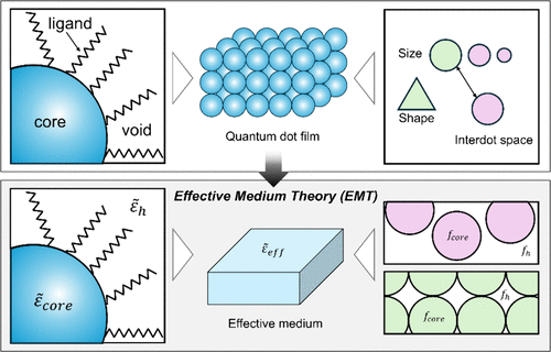
Figure 1. Effective-medium view of CQD films. Top: A heterogeneous CQD film comprises inorganic CQD cores, organic ligands, and interparticle voids; microstructural attributes─core size/shape and interdot spacing─govern packing. Bottom: In EMT, the film is replaced by a homogeneous medium with complex permittivity (ε̃eff); the CQD cores (ε̃core) act as inclusions embedded in a host of ligands and voids (ε̃h). The volume fractions fcore and fh encode the microstructure; the panels on the right illustrate different volume fractions.
Figure 2
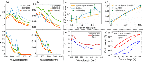
Figure 2. Complex refractive index of the CdSe cores and CdSe/CdS core–shell nanocrystals extracted in solution (a) and thin films (b). Adapted with permission from ref (35). Copyright 2018 American Chemical Society. The average refractive index of PbS CQD films from ellipsometry (symbols) and fNC (blue), obtained by fitting the ellipsometry data using the Bruggeman model or by a hard-sphere model (orange), plotted as a function of the PbS CQD excitonic peak (c) and surface ligand (d). Adapted with permission from ref (38). Copyright 2022 Royal Society of Chemistry. Real part of the effective dielectric function (e) and transfer curve (f) for InAs CQD films composed of tetrahedra (red) or spheres (blue) with identical particle volume (32 nm3). Adapted from ref (42) under the CC BY-NC-ND license. Copyright 2024 American Chemical Society.
Figure 3

Figure 3. (a) Multilayer CQD photodiode (TCO/ETL/CQD absorber/HTL/metal) forming a FP cavity. (b) TMM: each layer with thickness di and complex index Ñi represented by Mi. The total transfer matrix (M) relates to the incident and reflected fields. (c) Simulated electric-field intensity (|E| 2) vs wavelength (1100–1600 nm) and position. A resonance near 1.3 μm concentrates the field in the CQD layer. (d) Calculated nanocrystal absorption vs CQD film thickness and wavelength. Slanted bands are FP resonances. Adapted with permission from ref (38). Copyright 2022 Royal Society of Chemistry.
Figure 4

Figure 4. Thickness optimization of CQD absorbers. (a) PbS SWIR PD: TMM absorptance at the excitonic peak vs active-layer thickness (black) with measured EQE at 1550 nm under −2 V (red). Data from ref (47). (b) Micrometer-thick PbS CQD solar cell: EQE (purple) with the AM1.5G spectrum (gray). Adapted with permission from ref (50). Copyright 2020 American Chemical Society. (c) InAs NIR PD: TMM absorptance vs film thickness with representative reported EQEs (colored symbols). (d) Expected EQE from TMM (black) vs measured EQE (red circles) at 940 nm. (e) Thickness and bias dependent EQE (f) Specific detectivity at −1 V vs thickness (inset, EQE spectra). Adapted with permission from ref (51). Copyright 2024 Wiley-VCH GMbH.
Figure 5
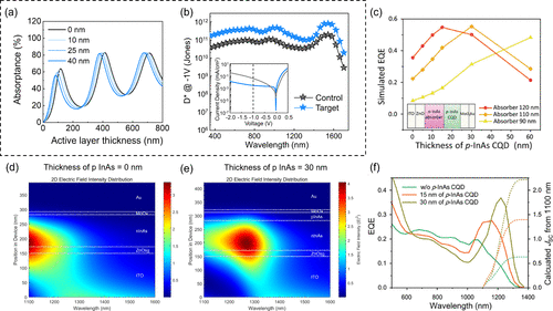
Figure 5. Optical-spacer engineering in CQD photodiodes. PbS SWIR PD with a MoOx IBL: (a) Simulated absorptance vs active-layer thickness for MoOx = 0, 10, 25, and 40 nm. (b) Specific detectivity at −1 V and dark current–voltage characteristics (inset) for devices with MoOx (black) and without MoOx (blue). Adapted with permission from ref (47). Copyright 2025 American Chemical Society. InAs CQD IR solar cell with a p-type optical spacer: (c) Simulated EQE vs p-InAs thickness for n-type absorber thicknesses of 90, 110, and 120 nm. 2D electric-field-intensity maps without (d) and with a 30 nm p-InAs layer (e). (f) Measured EQE (solid) for p-InAs thickness = 0, 15, and 30 nm and calculated integrated Jsc. Adapted with permission from ref (52). Copyright 2024 Wiley-VCH GMbH.
Figure 6

Figure 6. Advanced electrode designs for IR CQD solar cells. DBR cavity: (a) Schematic of reflective top contact and a DBR mirror contact, forming an optical cavity that enhances IR multipass. (b) EQE of the cavity device (red) versus a control without the cavity (black), showing enhancement near 1.3 μm. Adapted with permission from ref (53). Copyright 2016 American Chemical Society. Transparent IMZ electrode: (c) Transmittance of the IMZ asymmetric multilayer (red) compared with ITO (black dashed) over 1000–1800 nm at comparable sheet resistance (≈10 Ω sq–1); inset: IMZ stack. (d) EQE with ITO (black dashed), IMZ without Ag (yellow), and IMZ (red), demonstrating performance gains from the multilayer electrode. Adapted with permission from ref (54). Copyright 2018 American Chemical Society.
References
This article references 80 other publications.
- 1Karani, A.; Yang, L.; Bai, S.; Futscher, M. H.; Snaith, H. J.; Ehrler, B.; Greenham, N. C.; Di, D. Perovskite/colloidal quantum dot tandem solar cells: theoretical modeling and monolithic structure. ACS Energy Lett. 2018, 3 (4), 869– 874, DOI: 10.1021/acsenergylett.8b00207There is no corresponding record for this reference.
- 2Semonin, O. E.; Luther, J. M.; Beard, M. C. Quantum dots for next-generation photovoltaics. Mater. Today 2012, 15 (11), 508– 515, DOI: 10.1016/S1369-7021(12)70220-1There is no corresponding record for this reference.
- 3Cao, F.; Liu, L.; Li, L. Short-wave infrared photodetector. Mater. Today 2023, 62, 327– 349, DOI: 10.1016/j.mattod.2022.11.003There is no corresponding record for this reference.
- 4Wiley, L.; Cavanaugh, R.; Follansbee, J.; Burrell, D.; Grimming, R.; Pimpinella, R.; Voss, J.; Furxhi, O.; Driggers, R. Comparison of reflective band (Vis, NIR, SWIR, eSWIR) performance in daytime reduced illumination conditions. Appl. Opt. 2023, 62 (31), 8316– 8326, DOI: 10.1364/AO.495832There is no corresponding record for this reference.
- 5Polman, A.; Knight, M.; Garnett, E. C.; Ehrler, B.; Sinke, W. C. Photovoltaic materials: Present efficiencies and future challenges. Science 2016, 352 (6283), aad4424, DOI: 10.1126/science.aad4424There is no corresponding record for this reference.
- 6Sargent, E. H. Solar cells, photodetectors, and optical sources from infrared colloidal quantum dots. Adv. Mater. 2008, 20 (20), 3958– 3964, DOI: 10.1002/adma.200801153There is no corresponding record for this reference.
- 7García de Arquer, F. P.; Talapin, D. V.; Klimov, V. I.; Arakawa, Y.; Bayer, M.; Sargent, E. H. Semiconductor quantum dots: Technological progress and future challenges. Science 2021, 373 (6555), eaaz8541 DOI: 10.1126/science.aaz8541There is no corresponding record for this reference.
- 8Kim, M.; Choi, M.; Choi, S.; Jeong, S. Semiconductor nanocrystals: Unveiling the chemistry behind different facets. Acc. Chem. Res. 2023, 56 (13), 1756– 1765, DOI: 10.1021/acs.accounts.3c00123There is no corresponding record for this reference.
- 9Pinna, J.; Mehrabi Koushki, R.; Gavhane, D. S.; Ahmadi, M.; Mutalik, S.; Zohaib, M.; Protesescu, L.; Kooi, B. J.; Portale, G.; Loi, M. A. Approaching bulk mobility in PbSe colloidal quantum dots 3D superlattices. Adv. Mater. 2023, 35 (8), 2207364, DOI: 10.1002/adma.202207364There is no corresponding record for this reference.
- 10Kagan, C. R.; Murray, C. B. Charge transport in strongly coupled quantum dot solids. Nat. Nanotechnol. 2015, 10 (12), 1013– 1026, DOI: 10.1038/nnano.2015.247There is no corresponding record for this reference.
- 11Liu, Y.; Gibbs, M.; Puthussery, J.; Gaik, S.; Ihly, R.; Hillhouse, H. W.; Law, M. Dependence of carrier mobility on nanocrystal size and ligand length in PbSe nanocrystal solids. Nano Lett. 2010, 10 (5), 1960– 1969, DOI: 10.1021/nl101284kThere is no corresponding record for this reference.
- 12Bederak, D.; Balazs, D. M.; Sukharevska, N. V.; Shulga, A. G.; Abdu-Aguye, M.; Dirin, D. N.; Kovalenko, M. V.; Loi, M. A. Comparing halide ligands in PbS colloidal quantum dots for field-effect transistors and solar cells. ACS Appl. Nano Mater. 2018, 1 (12), 6882– 6889, DOI: 10.1021/acsanm.8b01696There is no corresponding record for this reference.
- 13Septianto, R. D.; Miranti, R.; Kikitsu, T.; Hikima, T.; Hashizume, D.; Matsushita, N.; Iwasa, Y.; Bisri, S. Z. Enabling metallic behaviour in two-dimensional superlattice of semiconductor colloidal quantum dots. Nat. Commun. 2023, 14, 2670, DOI: 10.1038/s41467-023-38216-yThere is no corresponding record for this reference.
- 14Choi, M.; Kim, M.; Lee, Y.; Kim, T.; Kim, J. H.; Shin, D.; Kim, J. W.; Kim, Y. H.; Jeong, S. Tailored band edge positions by fractional ligand replacement of nonconductive colloidal quantum dot films. J. Phys. Chem. C 2023, 127 (9), 4825– 4832, DOI: 10.1021/acs.jpcc.3c00376There is no corresponding record for this reference.
- 15Kroupa, D. M.; Vörös, M.; Brawand, N. P.; McNichols, B. W.; Miller, E. M.; Gu, J.; Nozik, A. J.; Sellinger, A.; Galli, G.; Beard, M. C. Tuning colloidal quantum dot band edge positions through solution-phase surface chemistry modification. Nat. Commun. 2017, 8, 15257, DOI: 10.1038/ncomms15257There is no corresponding record for this reference.
- 16Song, J. H.; Choi, H.; Pham, H. T.; Jeong, S. Energy level tuned indium arsenide colloidal quantum dot films for efficient photovoltaics. Nat. Commun. 2018, 9, 4267, DOI: 10.1038/s41467-018-06399-4There is no corresponding record for this reference.
- 17Brown, P. R.; Kim, D.; Lunt, R. R.; Zhao, N.; Bawendi, M. G.; Grossman, J. C.; Bulović, V. Energy level modification in lead sulfide quantum dot thin films through ligand exchange. ACS Nano 2014, 8 (6), 5863– 5872, DOI: 10.1021/nn500897cThere is no corresponding record for this reference.
- 18Chehaibou, B.; Reiss, P.; Lhuillier, E.; Mugny, G.; Delerue, C.; Arnaud, A. Colloidal quantum dots thin films: A theoretical insight into optical efficiency for optoelectronic applications. IEEE Trans. Electron Devices 2025, 72 (2), 712– 722, DOI: 10.1109/TED.2024.3517595There is no corresponding record for this reference.
- 19Nayak, J. K.; Chaudhuri, P. R.; Ratha, S.; Sahoo, M. R. A comprehensive review on effective medium theories to find effective dielectric constant of composites. J. Electromagn. Waves Appl. 2023, 37 (2), 282– 322, DOI: 10.1080/09205071.2022.2135029There is no corresponding record for this reference.
- 20Konstantatos, G.; Sargent, E. H. Colloidal quantum dot photodetectors. Infrared Phys. Technol. 2011, 54 (3), 278– 282, DOI: 10.1016/j.infrared.2010.12.029There is no corresponding record for this reference.
- 21Lin, W. M. M.; Yazdani, N.; Yarema, O.; Yarema, M.; Liu, M.; Sargent, E. H.; Kirchartz, T.; Wood, V. Recombination dynamics in PbS nanocrystal quantum dot solar cells studied through drift–diffusion simulations. ACS Appl. Electron. Mater. 2021, 3 (11), 4977– 4989, DOI: 10.1021/acsaelm.1c00787There is no corresponding record for this reference.
- 22Clifford, J. P.; Konstantatos, G.; Johnston, K. W.; Hoogland, S.; Levina, L.; Sargent, E. H. Fast, sensitive and spectrally tuneable colloidal-quantum-dot photodetectors. Nat. Nanotechnol. 2009, 4 (1), 40– 44, DOI: 10.1038/nnano.2008.313There is no corresponding record for this reference.
- 23Chuang, C. H. M.; Brown, P. R.; Bulović, V.; Bawendi, M. G. Improved performance and stability in quantum dot solar cells through band alignment engineering. Nat. Mater. 2014, 13 (8), 796– 801, DOI: 10.1038/nmat3984There is no corresponding record for this reference.
- 24Zhitomirsky, D.; Voznyy, O.; Levina, L.; Hoogland, S.; Kemp, K. W.; Ip, A. H.; Thon, S. M.; Sargent, E. H. Engineering colloidal quantum dot solids within and beyond the mobility-invariant regime. Nat. Commun. 2014, 5, 3803, DOI: 10.1038/ncomms4803There is no corresponding record for this reference.
- 25Lim, C.; Choi, M.; Kim, T.; Shin, D.; Song, J. H.; Jeong, S. Effect of bandgap variation on photovoltaic properties of lead sulfide quantum dot solar cell. Mater. Today Energy 2023, 36, 101357, DOI: 10.1016/j.mtener.2023.101357There is no corresponding record for this reference.
- 26Li, M.; Yan, J.; Zhao, X.; Ma, T.; Zhang, A.; Chen, S.; Shen, G.; Khalaf, G. M. G.; Zhang, J.; Chen, C.; Hsu, H. Y.; Song, H.; Yang, P.; Tang, J. Synergistic enhancement of efficient perovskite/quantum dot tandem solar cells based on transparent electrode and band alignment engineering. Adv. Energy Mater. 2024, 14 (23), 2400219, DOI: 10.1002/aenm.202400219There is no corresponding record for this reference.
- 27Valiei, M.; Shaibani, P. M.; Abdizadeh, H.; Kolahdouz, M.; Asl Soleimani, E.; Poursafar, J. Design and optimization of single, double and multilayer anti-reflection coatings on planar and textured surface of silicon solar cells. Mater. Today Commun. 2022, 32, 104144, DOI: 10.1016/j.mtcomm.2022.104144There is no corresponding record for this reference.
- 28Beyer, B.; Leo, K. Efficiency increase of organic solar cells with emissive light-in-coupling layers. J. Mater. Chem. C 2015, 3 (41), 10830– 10836, DOI: 10.1039/C5TC02446CThere is no corresponding record for this reference.
- 29Kholmicheva, N.; Moroz, P.; Rijal, U.; Bastola, E.; Uprety, P.; Liyanage, G.; Razgoniaev, A.; Ostrowski, A. D.; Zamkov, M. Plasmonic nanocrystal solar cells utilizing strongly confined radiation. ACS Nano 2014, 8 (12), 12549– 12559, DOI: 10.1021/nn505375nThere is no corresponding record for this reference.
- 30Hong, J.; Kim, B. S.; Hou, B.; Cho, Y.; Lee, S. H.; Pak, S.; Morris, S. M.; Sohn, J. I.; Cha, S. N. Plasmonic effects of dual-metal nanoparticle layers for high-performance quantum dot solar cells. Plasmonics 2020, 15 (4), 1007– 1013, DOI: 10.1007/s11468-020-01120-yThere is no corresponding record for this reference.
- 31Tabernig, S. W.; Yuan, L.; Cordaro, A.; Teh, Z. L.; Gao, Y.; Patterson, R. J.; Pusch, A.; Huang, S.; Polman, A. Optically resonant bulk heterojunction PbS quantum dot solar cell. ACS Nano 2022, 16 (9), 13750– 13760, DOI: 10.1021/acsnano.1c11330There is no corresponding record for this reference.
- 32Labelle, A. J.; Thon, S. M.; Masala, S.; Adachi, M. M.; Dong, H.; Farahani, M.; Ip, A. H.; Fratalocchi, A.; Sargent, E. H. Colloidal quantum dot solar cells exploiting hierarchical structuring. Nano Lett. 2015, 15 (2), 1101– 1108, DOI: 10.1021/nl504086vThere is no corresponding record for this reference.
- 33Kim, T.; Jin, X.; Song, J. H.; Jeong, S.; Park, T. Efficiency limit of colloidal quantum dot solar cells: effect of optical interference on active layer absorption. ACS Energy Lett. 2020, 5 (1), 248– 251, DOI: 10.1021/acsenergylett.9b02504There is no corresponding record for this reference.
- 34Markel, V. A. Introduction to the Maxwell Garnett approximation: tutorial. J. Opt. Soc. Am. A 2016, 33 (7), 1244– 1256, DOI: 10.1364/JOSAA.33.001244There is no corresponding record for this reference.
- 35Dement, D. B.; Puri, M.; Ferry, V. E. Determining the complex refractive index of neat CdSe/CdS quantum dot films. J. Phys. Chem. C 2018, 122 (37), 21557– 21568, DOI: 10.1021/acs.jpcc.8b04522There is no corresponding record for this reference.
- 36Grinolds, D. D. W.; Brown, P. R.; Harris, D. K.; Bulović, V.; Bawendi, M. G. Quantum-dot size and thin-film dielectric constant: precision measurement and disparity with simple models. Nano Lett. 2015, 15 (1), 21– 26, DOI: 10.1021/nl5024244There is no corresponding record for this reference.
- 37Murray, C. B.; Kagan, C. R.; Bawendi, M. G. Synthesis and characterization of monodisperse nanocrystals and close-packed nanocrystal assemblies. Annu. Rev. Mater. Sci. 2000, 30 (1), 545– 610, DOI: 10.1146/annurev.matsci.30.1.545There is no corresponding record for this reference.
- 38Chehaibou, B.; Izquierdo, E.; Chu, A.; Abadie, C.; Cavallo, M.; Khalili, A.; Dang, T. H.; Gréboval, C.; Xu, X. Z.; Ithurria, S.; Vincent, G.; Gallas, B.; Mugny, G.; Arnaud, A.; Lhuillier, E.; Delerue, C. The complex optical index of PbS nanocrystal thin films and their use for short wave infrared sensor design. Nanoscale 2022, 14 (7), 2711– 2721, DOI: 10.1039/D1NR07770HThere is no corresponding record for this reference.
- 39Diroll, B. T.; Gaulding, E. A.; Kagan, C. R.; Murray, C. B. Spectrally-resolved dielectric functions of solution-cast quantum dot thin films. Chem. Mater. 2015, 27 (18), 6463– 6469, DOI: 10.1021/acs.chemmater.5b02953There is no corresponding record for this reference.
- 40Zhang, Z.; Thung, Y. T.; Chen, X.; Wang, L.; Fan, W.; Ding, L.; Sun, H. Study of complex optical constants of neat cadmium selenide nanoplatelets thin films by spectroscopic ellipsometry. J. Phys. Chem. Lett. 2021, 12 (1), 191– 198, DOI: 10.1021/acs.jpclett.0c03304There is no corresponding record for this reference.
- 41Rastogi, P.; Chu, A.; Dang, T. H.; Prado, Y.; Gréboval, C.; Qu, J.; Dabard, C.; Khalili, A.; Dandeu, E.; Fix, B.; Xu, X. Z.; Ithurria, S.; Vincent, G.; Gallas, B.; Lhuillier, E. Complex optical index of HgTe nanocrystal infrared thin films and its use for short-wave infrared photodiode design. Adv. Opt. Mater. 2021, 9 (10), 2002066, DOI: 10.1002/adom.202002066There is no corresponding record for this reference.
- 42Kim, M.; Lee, J.; Jung, J.; Shin, D.; Kim, J.; Cho, E.; Xing, Y.; Jeong, H.; Park, S.; Oh, S. H.; Kim, Y. H.; Jeong, S. Surface-originated weak confinement in tetrahedral indium arsenide quantum dots. J. Am. Chem. Soc. 2024, 146 (15), 10251– 10256, DOI: 10.1021/jacs.4c00966There is no corresponding record for this reference.
- 43Pettersson, L. A. A.; Roman, L. S.; Inganäs, O. Modeling photocurrent action spectra of photovoltaic devices based on organic thin films. J. Appl. Phys. 1999, 86 (1), 487– 496, DOI: 10.1063/1.370757There is no corresponding record for this reference.
- 44Burkhard, G. F.; Hoke, E. T.; McGehee, M. D. Accounting for interference, scattering, and electrode absorption to make accurate internal quantum efficiency measurements in organic and other thin solar cells. Adv. Mater. 2010, 22 (30), 3293– 3297, DOI: 10.1002/adma.201000883There is no corresponding record for this reference.
- 45Luce, A.; Mahdavi, A.; Marquardt, F.; Wankerl, H. TMM-Fast, a transfer matrix computation package for multilayer thin-film optimization: tutorial. J. Opt. Soc. Am. A 2022, 39 (6), 1007– 1013, DOI: 10.1364/JOSAA.450928There is no corresponding record for this reference.
- 46Ouellette, O.; Lesage-Landry, A.; Scheffel, B.; Hoogland, S.; García de Arquer, F. P.; Sargent, E. H. Spatial collection in colloidal quantum dot solar cells. Adv. Funct. Mater. 2020, 30 (1), 1908200, DOI: 10.1002/adfm.201908200There is no corresponding record for this reference.
- 47Tran, H. C. V.; Jang, E.; Kim, J.; Choi, M.; Park, Y.; Jeong, H.; Goo, T.; Bae, S.; Jeong, S. Enhanced SWIR photodetection in colloidal quantum dot photodiodes via tunneling current suppression. ACS Appl. Mater. Interfaces 2025, 17 (10), 15666– 15674, DOI: 10.1021/acsami.4c22853There is no corresponding record for this reference.
- 48Huang, Y.; Hao, L.; Shao, L.; Tan, Z.; Li, S.; Dong, S.; Yang, X.; Zhong, W.; Wang, Y.; Huang, F. Near-infrared organic photodetectors with tailored junction thickness for resonance-enhanced photoresponse and suppressed dark current. ACS Photonics 2025, 12 (7), 3928– 3938, DOI: 10.1021/acsphotonics.5c01055There is no corresponding record for this reference.
- 49Ooi, Z. Y.; Nie, S.; Vega, G.; Lai, M. C.; Jiménez-Solano, A.; Huang, C. S.; Wang, H.; Liu, T.; Gałkowski, K.; Nowak, M. P.; Nyga, P.; Cheng, Q.; Ducati, C.; Carretero-Palacios, S.; Kahmann, S.; Stranks, S. D.; Anaya, M. Resonant cavity effect for spectrally tunable and efficient narrowband perovskite photodetectors. ACS Photonics 2025, 12 (8), 4119– 4129, DOI: 10.1021/acsphotonics.4c01942There is no corresponding record for this reference.
- 50Fan, J. Z.; Vafaie, M.; Bertens, K.; Sytnyk, M.; Pina, J. M.; Sagar, L. K.; Ouellette, O.; Proppe, A. H.; Rasouli, A. S.; Gao, Y.; Baek, S. W.; Chen, B.; Laquai, F.; Hoogland, S.; De Arquer, F. P. G.; Heiss, W.; Sargent, E. H. Micron thick colloidal quantum dot solids. Nano Lett. 2020, 20 (7), 5284– 5291, DOI: 10.1021/acs.nanolett.0c01614There is no corresponding record for this reference.
- 51Shin, D.; Jeong, H.; Kim, J.; Jang, E.; Park, Y.; Jeong, S. High-performance infrared InAs colloidal quantum dot photodetector with 79% EQE enabled by an extended absorber layer. Adv. Opt. Mater. 2025, 13 (1), 2401931, DOI: 10.1002/adom.202401931There is no corresponding record for this reference.
- 52Park, Y.; Kim, J.; Jeong, M.; Shin, D.; Jung, J.; Kim, H.; Jeong, H.; Kim, H.; Kim, Y. H.; Jeong, S. Pb-free infrared harvesting colloidal quantum dot solar cells using n–p homojunction architecture. Adv. Energy Mater. 2025, 15 (11), 2404141, DOI: 10.1002/aenm.202404141There is no corresponding record for this reference.
- 53Ouellette, O.; Hossain, N.; Sutherland, B. R.; Kiani, A.; García de Arquer, F. P.; Tan, H.; Chaker, M.; Hoogland, S.; Sargent, E. H. Optical resonance engineering for infrared colloidal quantum dot photovoltaics. ACS Energy Lett. 2016, 1 (4), 852– 857, DOI: 10.1021/acsenergylett.6b00403There is no corresponding record for this reference.
- 54Baek, S. W.; Ouellette, O.; Jo, J. W.; Choi, J.; Seo, K. W.; Kim, J.; Sun, B.; Lee, S. H.; Choi, M. J.; Nam, D. H.; Quan, L. N.; Kang, J.; Hoogland, S.; García de Arquer, F. P.; Lee, J. Y.; Sargent, E. H. Infrared cavity-enhanced colloidal quantum dot photovoltaics employing asymmetric multilayer electrodes. ACS Energy Lett. 2018, 3 (12), 2908– 2913, DOI: 10.1021/acsenergylett.8b01878There is no corresponding record for this reference.
- 55Hens, Z.; Moreels, I. Light absorption by colloidal semiconductor quantum dots. J. Mater. Chem. 2012, 22 (21), 10406– 10415, DOI: 10.1039/c2jm30760jThere is no corresponding record for this reference.
- 56Delerue, C.; Allan, G.; Lannoo, M. Concept of dielectric constant for nanosized systems. Phys. Rev. B 2003, 68 (11), 115411, DOI: 10.1103/PhysRevB.68.115411There is no corresponding record for this reference.
- 57Delerue, C.; Lannoo, M.; Allan, G. Tight binding for complex semiconductor systems. Phys. Status Solidi B 2001, 227 (1), 115– 149, DOI: 10.1002/1521-3951(200109)227:1<115::AID-PSSB115>3.0.CO;2-2There is no corresponding record for this reference.
- 58Chehaibou, B.; Abadie, C.; Prado, Y.; Xu, X. Z.; Vincent, G.; Gallas, B.; Mugny, G.; Arnaud, A.; Lhuillier, E.; Delerue, C. Modeling HgTe complex optical index from bulk to nanocrystal layers. J. Phys. Chem. C 2023, 127 (28), 13789– 13799, DOI: 10.1021/acs.jpcc.3c01837There is no corresponding record for this reference.
- 59Kim, T.; Shin, D.; Kim, M.; Kim, H.; Cho, E.; Choi, M.; Kim, J.; Jang, E.; Jeong, S. Development of group III–V colloidal quantum dots for optoelectronic applications. ACS Energy Lett. 2023, 8 (1), 447– 456, DOI: 10.1021/acsenergylett.2c02489There is no corresponding record for this reference.
- 60Shin, D.; Park, Y.; Jeong, H.; Tran, H. C. V.; Jang, E.; Jeong, S. Exploring the potential of colloidal quantum dots for near-infrared to short-wavelength infrared applications. Adv. Energy Mater. 2025, 15, 2304550, DOI: 10.1002/aenm.202304550There is no corresponding record for this reference.
- 61Kim, Y.; Chang, J. H.; Choi, H.; Kim, Y.-H.; Bae, W. K.; Jeong, S. III–V colloidal nanocrystals: Control of covalent surfaces. Chem. Sci. 2020, 11 (4), 913– 922, DOI: 10.1039/C9SC04290CThere is no corresponding record for this reference.
- 62Wolcott, A.; Doyeux, V.; Nelson, C. A.; Gearba, R.; Lei, K. W.; Yager, K. G.; Dolocan, A. D.; Williams, K.; Nguyen, D.; Zhu, X. Y. Anomalously large polarization effect responsible for excitonic red shifts in PbSe quantum dot solids. J. Phys. Chem. Lett. 2011, 2 (7), 795– 800, DOI: 10.1021/jz200080dThere is no corresponding record for this reference.
- 63Vossmeyer, T.; Katsikas, L.; Giersig, M.; Popovic, I. G.; Diesner, K.; Chemseddine, A.; Eychmüller, A.; Weller, H. CdS nanoclusters: Synthesis, characterization, size-dependent oscillator strength, temperature shift of the excitonic transition energy, and reversible absorbance shift. J. Phys. Chem. 1994, 98 (31), 7665– 7673, DOI: 10.1021/j100082a044There is no corresponding record for this reference.
- 64Kagan, C. R.; Murray, C. B.; Bawendi, M. G. Long-range resonance transfer of electronic excitations in close-packed CdSe quantum-dot solids. Phys. Rev. B 1996, 54 (12), 8633– 8643, DOI: 10.1103/PhysRevB.54.8633There is no corresponding record for this reference.
- 65Kagan, C. R.; Murray, C. B.; Nirmal, M.; Bawendi, M. G. Electronic energy transfer in CdSe quantum dot solids. Phys. Rev. Lett. 1996, 76 (9), 1517– 1520, DOI: 10.1103/PhysRevLett.76.1517There is no corresponding record for this reference.
- 66Leatherdale, C. A.; Bawendi, M. G. Observation of solvatochromism in CdSe colloidal quantum dots. Phys. Rev. B 2001, 63 (16), 165315, DOI: 10.1103/PhysRevB.63.165315There is no corresponding record for this reference.
- 67Lee, T. G.; Enomoto, K.; Ohshiro, K.; Inoue, D.; Kikitsu, T.; Hyeon-Deuk, K.; Pu, Y. J.; Kim, D. G. Controlling the dimension of the quantum resonance in CdTe quantum dot superlattices fabricated via layer-by-layer assembly. Nat. Commun. 2020, 11, 5471, DOI: 10.1038/s41467-020-19337-0There is no corresponding record for this reference.
- 68Williams, K. J.; Tisdale, W. A.; Leschkies, K. S.; Haugstad, G.; Norris, D. J.; Aydil, E. S.; Zhu, X. Y. Strong electronic coupling in two-dimensional assemblies of colloidal PbSe quantum dots. ACS Nano 2009, 3 (6), 1532– 1538, DOI: 10.1021/nn9001819There is no corresponding record for this reference.
- 69Geiregat, P.; Justo, Y.; Abe, S.; Flamee, S.; Hens, Z. Giant and broadband absorption enhancement in colloidal quantum dot monolayers through dipolar coupling. ACS Nano 2013, 7 (2), 987– 993, DOI: 10.1021/nn305524aThere is no corresponding record for this reference.
- 70Sukhov, S.; Haefner, D.; Dogariu, A. Coupled dipole method for modeling optical properties of large-scale random media. Phys. Rev. E 2008, 77 (6), 066709, DOI: 10.1103/PhysRevE.77.066709There is no corresponding record for this reference.
- 71Zhang, X.; Wu, Y. Effective medium theory for anisotropic metamaterials. Sci. Rep. 2015, 5, 7892, DOI: 10.1038/srep07892There is no corresponding record for this reference.
- 72Granqvist, C. G.; Hunderi, O. Conductivity of inhomogeneous materials: Effective-medium theory with dipole–dipole interaction. Phys. Rev. B 1978, 18 (4), 1554– 1561, DOI: 10.1103/PhysRevB.18.1554There is no corresponding record for this reference.
- 73Zhao, X.; Wang, J.; Liu, M.; Ma, X.; Zhang, F. Narrowband organic photodetectors: From fundamentals to prospects. Adv. Opt. Mater. 2024, 12, 2401087, DOI: 10.1002/adom.202401087There is no corresponding record for this reference.
- 74Wang, Y.; Kublitski, J.; Xing, S.; Dollinger, F.; Spoltore, D.; Benduhn, J.; Leo, K. Narrowband organic photodetectors─towards miniaturized, spectroscopic sensing. Mater. Horiz. 2022, 9 (1), 220– 251, DOI: 10.1039/D1MH01215KThere is no corresponding record for this reference.
- 75Pina, J. M.; Vafaie, M.; Parmar, D. H.; Atan, O.; Xia, P.; Zhang, Y.; Najarian, A. M.; De Arquer, F. P. G.; Hoogland, S.; Sargent, E. H. Quantum-size-effect tuning enables narrowband IR photodetection with low sunlight interference. Nano Lett. 2022, 22 (16), 6802– 6807, DOI: 10.1021/acs.nanolett.2c02756There is no corresponding record for this reference.
- 76Song, J. H.; Kim, J.; Kim, M.; Park, J.-G.; Kang, J.-W. Tunable infrared Bragg reflectors of entirely ligand-engineered lead sulfide quantum dot layers. J. Phys. Chem. C 2025. DOI: 10.1021/acs.jpcc.5c06300 .There is no corresponding record for this reference.
- 77Palo, E.; Daskalakis, K. S. Prospects in broadening the application of planar solution-based distributed Bragg reflectors. Adv. Mater. Interfaces 2023, 10, 2202206, DOI: 10.1002/admi.202202206There is no corresponding record for this reference.
- 78Lova, P.; Manfredi, G.; Comoretto, D. Advances in functional solution-processed planar 1D photonic crystals. Adv. Opt. Mater. 2018, 6, 1800730, DOI: 10.1002/adom.201800730There is no corresponding record for this reference.
- 79Palo, E.; Papachatzakis, M. A.; Abdelmagid, A.; Qureshi, H.; Kumar, M.; Salomäki, M.; Daskalakis, K. S. Developing solution-processed distributed Bragg reflectors for microcavity polariton applications. J. Phys. Chem. C 2023, 127 (29), 14255– 14262, DOI: 10.1021/acs.jpcc.3c01457There is no corresponding record for this reference.
- 80Chen, Y. C.; Yeh, H.; Lee, C. J.; Chang, W. H. Distributed Bragg reflectors as broadband and large-area platforms for light-coupling enhancement in 2D transition-metal dichalcogenides. ACS Appl. Mater. Interfaces 2018, 10 (19), 16874– 16880, DOI: 10.1021/acsami.8b02845There is no corresponding record for this reference.