


This publication is free to access through this site. Learn More

ACS Editors' Choice® is a collection designed to feature scientific articles of broad public interest. Read the latest articles
Harnessing Plateau–Rayleigh Instability in GeS Nanowires for Nanoscale Optoelectronic HeterojunctionsClick to copy article linkArticle link copied!
- Seong Bin ParkSeong Bin ParkProgram in Biomedical Science and Engineering, Inha University, Incheon 22212, Republic of KoreaProgram in Energy Process Innovation Convergence, Inha University, Incheon 22212, Republic of KoreaMore by Seong Bin Park
- Yujin KongYujin KongProgram in Biomedical Science and Engineering, Inha University, Incheon 22212, Republic of KoreaProgram in Energy Process Innovation Convergence, Inha University, Incheon 22212, Republic of KoreaMore by Yujin Kong
- Yu Chan WonYu Chan WonProgram in Biomedical Science and Engineering, Inha University, Incheon 22212, Republic of KoreaProgram in Energy Process Innovation Convergence, Inha University, Incheon 22212, Republic of KoreaMore by Yu Chan Won
- Naechul Shin*Naechul Shin*Email: [email protected]Program in Biomedical Science and Engineering, Inha University, Incheon 22212, Republic of KoreaProgram in Energy Process Innovation Convergence, Inha University, Incheon 22212, Republic of KoreaDepartment of Chemical Engineering, Inha University, Incheon 22212, Republic of KoreaMore by Naechul Shin
Abstract
Periodic shell formation in one-dimensional structures is a classical outcome of the Plateau–Rayleigh (P-R) instability, yet its manifestation in van der Waals (vdW) crystals has remained unexplored. Here, we demonstrate P-R instability in GeS vdW nanowires, synthesized by vapor–liquid–solid growth. Under elevated temperatures and continuous precursor supply, GeS nanowires transition from smooth sidewalls to periodic core–shell architectures. A quasi-liquid amorphous surface layer reorganizes into sulfur-rich shells surrounding a crystalline core. By tuning growth duration, both shell diameters and intershell pitches can be systematically controlled, consistent with theoretical predictions. Furthermore, these nanowires define site-specific nanoscale junctions in mixed-dimensional heterostructures. When integrated with monolayer WSe2, GeS shells create localized heterojunctions that drive charge transfer and excitonic modulation. Photoluminescence mapping and spectral analysis reveal exciton redshifts, trion enhancement, and localized quenching. These findings extend P-R instability to vdW materials and establish periodic nanowires as a platform for optoelectronic patterning.
This publication is licensed for personal use by The American Chemical Society.
Periodic Shell Formation on GeS Nanowires via P-R Instability
Figure 1
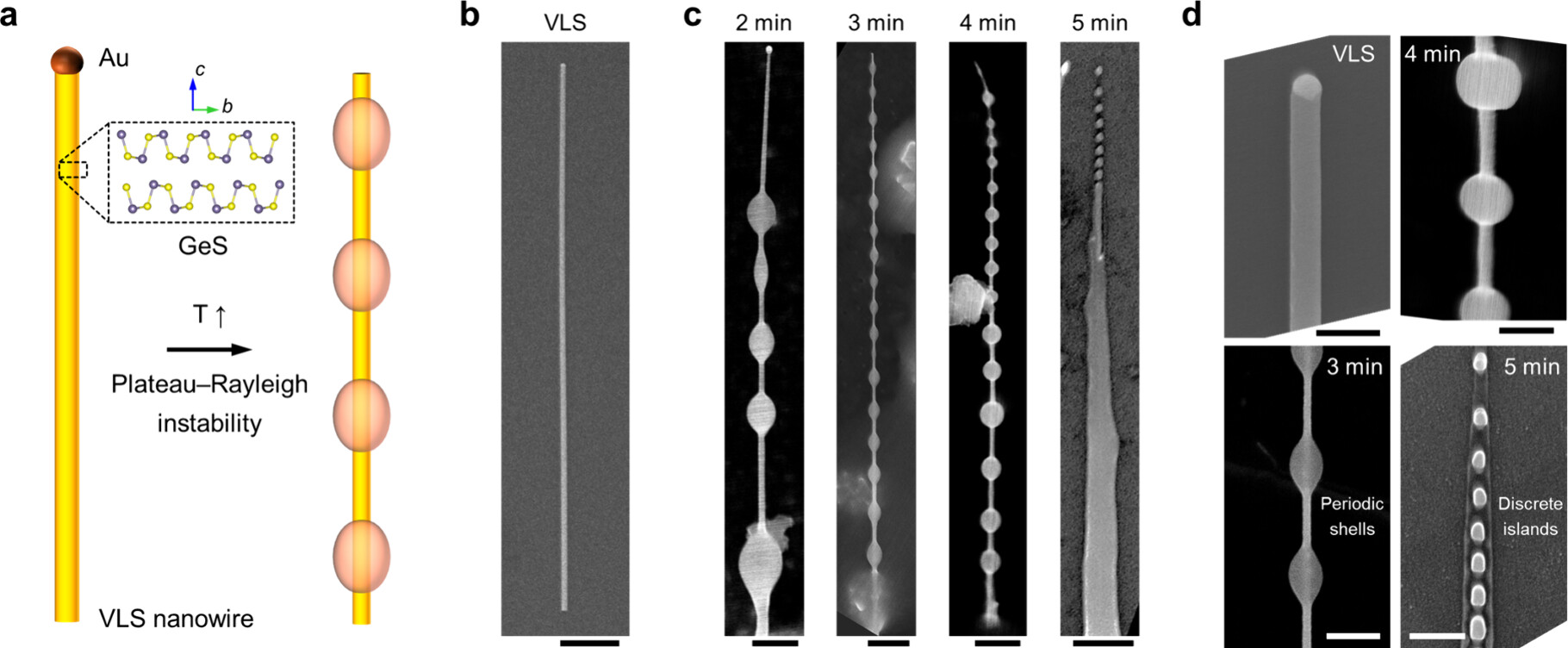
Figure 1. Periodic shell formation on a GeS van der Waals nanowire via the Plateau–Rayleigh (P-R) instability. (a) Schematic illustration showing the formation of a periodic core–shell GeS nanowire from a VLS-grown straight nanowire, driven by the P-R instability at elevated temperature. Inset highlights orthorhombic GeS crystal structure where the vdW layers are transversely stacked relative to the axial direction. (b) SEM image of a straight GeS nanowire grown from an Au catalyst. The growth was conducted by nucleating at 380 °C for 3 min and elongating at 300 °C for 10 min. The pressure and Ar carrier gas flow rate were 20 Torr and 50 sccm, respectively. Scale bar, 1 μm. (c) SEM images showing the evolution of periodic core–shell structure. The growth was continued at 390 °C, under a pressure of 20 Torr and an Ar gas flow rate of 50 sccm, for growth times (tg) of 2–5 min (from left to right). Scale bars, 500 nm. (d) Magnified SEM plan views of GeS nanowires. Top left: A straight VLS nanowire with its growth front decorated with an Au catalytic droplet. Bottom left and Top right: Core–shell structures showing periodic shells at tg = 3 and 4 min, respectively. Bottom right: Discrete islands formed by the P-R instability at tg = 5 min. Scale bars, 200 nm.
Structural Analysis of GeS Periodic Core–Shell Nanowires
Figure 2
Figure 2. Structural analysis of GeS periodic shell nanowires. (a) Bright-field TEM image of a GeS periodic shell nanowire (tg = 3 min). Scale bar, 500 nm. (b) Magnified TEM image of the region marked by the red square in (a). Scale bar, 200 nm. (c) High-resolution TEM image of the crystalline core and amorphous shell, corresponding to the area in the blue box region of the top-left inset. The image shows a lattice spacing of 0.53 nm and confirms the axial orientation is along the [001] direction. Bottom left inset: Corresponding SAED pattern from a [110] zone axis, validating the axial orientation along the c-axis. Scale bars, 10 nm (main image), 100 nm (top-left inset), and 100 nm–1. (d) EDS elemental mapping images of the GeS periodic shell nanowire. Scale bar, 500 nm.
Morphological Evolution during P-R Growth
Figure 3
Figure 3. Time-dependent periodic shell formation on GeS nanowire sidewalls. (a) SEM images showing the morphological evolution of GeS nanowire. A VLS nanowire with straight and uniform sidewall grown at 300 °C, periodic core–shell structures after growth for 2, 3, and 4 min at 390 °C (top to bottom). Scale bars, 500 nm. (b) AFM height map (top) and corresponding axial line profile (bottom) of a representative periodic core–shell nanowire with tg = 3 min. The profile shows a periodic height modulation superimposed on a gradual decrease in the average height from base (left) to tip (right). Scale bar, 1 μm. (c) Statistical distribution of the shell pitch as a function of growth time. (d) Nanowire (core) diameter (Dc, left axis) and the shell-to-core diameter ratio (Ds/Dc, right axis) as a function of growth time. The inset illustrates the definitions of these parameters. (e) Experimentally measured correlation between shell pitch and shell diameter for different growth times. The data are overlaid with a theoretical model prediction, where the solid red line indicates the thermodynamic threshold for spontaneous periodic shell formation (ΔGs < 0) for Dc = 50 nm and Dw = 100 nm, where Dw is the fictitious diameter of a conformal shell. (f) Theoretical stability diagram derived from the model, showing the calculated instability threshold as a function of shell diameter and pitch for various core and fictitious conformal shell diameters.
Localized Optoelectronic Modulation
Figure 4
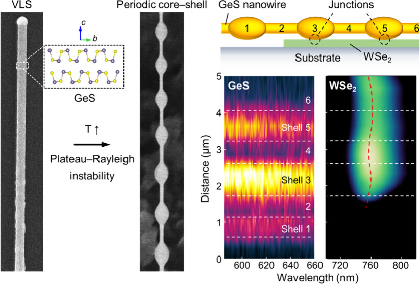
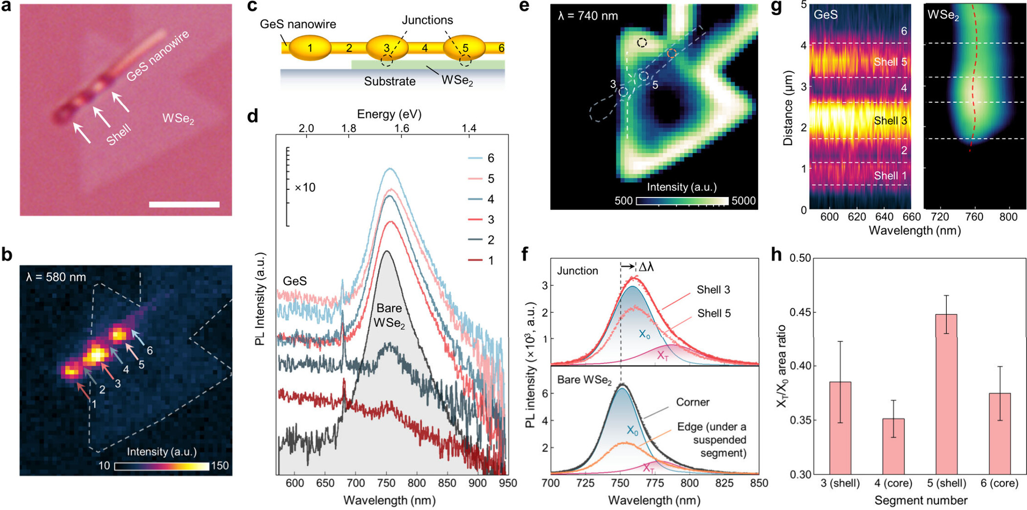
Figure 4. Spatially modulated optoelectronic properties of GeS/WSe2 mixed-dimensional vdW heterostructure. (a) OM image of a periodic core–shell GeS nanowire transferred onto a monolayer WSe2. Scale bar, 3 μm. (b) PL intensity map corresponding to the GeS emission (λ = 580 nm), showing emission is brightest at the shell segments (1, 3, 5). (c) Schematic illustration of the heterostructure, highlighting the direct vdW junctions formed between the GeS shells (i.e., 3, 5) and the underlying WSe2. (d) PL spectra from numbered nanowire points and a bare WSe2 region (black), showing broad GeS (λ ≤ 680 nm) and sharp WSe2 (∼750 nm) exciton peaks. Spectra are offset for clarity. (e) PL intensity map of the WSe2 emission (λ = 740 nm), confirming strong, localized PL quenching at the GeS shell junctions. Dashed circles indicate the locations of the spectra shown in (f). (f) Deconvoluted PL spectra from representative ‘Junction’ (top) and ‘Pristine’ (bottom) regions, as marked in (e). The peaks are fitted to a neutral exciton (X0) and a lower-energy trion (XT). The junction spectra exhibit a significant redshift (Δλ = 10 nm) and an enhanced trion contribution. (g) Spatially resolved hyperspectral maps along the nanowire axis, showing the direct correlation between the GeS PL intensity modulation and the redshift of the WSe2 PL at the shell junctions. Color scales are identical to those in (b) and (e). (h) Ratio of the integrated trion-to-exciton peak areas for junction segments located on the WSe2 flake, confirming a local enhancement of the trion population specifically at the shell junctions (3 and 5).
Supporting Information
The Supporting Information is available free of charge at https://pubs.acs.org/doi/10.1021/acs.nanolett.5c04385.
SEM image of Au nanoparticles dispersed on Si substrate and optical microscopic images of as-grown and dry-transferred GeS nanowires. TEM and EDS analyses of straight and core–shell nanowires. EDS spectra of core–shell GeS nanowires. Raman spectrum of a periodic core–shell GeS nanowire. Additional SEM images of periodic core–shell GeS nanowires at different growth durations. Statistical distributions of shell diameters and shell contact angles as a function of growth time. Comparison of shell-thicknesses measurements by AFM and SEM. Shell and core diameter comparison between upper and lower segments. Comparison of core and shell diameters at the upper and lower segments in periodic nanowires. Schematic comparing periodic shell and conformal shell structures. PL measurements on a core–shell GeS nanowire. PL spectra comparison between shell contact and intershell regions. UPS analysis of GeS. Superimposed PL intensity maps at the GeS and WSe2 emission wavelengths. PL peak deconvolution near the GeS/WSe2 junction regions. Comparison of P-R instability in nanowires reported in previous studies. (PDF)
Terms & Conditions
Most electronic Supporting Information files are available without a subscription to ACS Web Editions. Such files may be downloaded by article for research use (if there is a public use license linked to the relevant article, that license may permit other uses). Permission may be obtained from ACS for other uses through requests via the RightsLink permission system: http://pubs.acs.org/page/copyright/permissions.html.
Author Information
- Naechul Shin - Program in Biomedical Science and Engineering, Inha University, Incheon 22212, Republic of Korea; Program in Energy Process Innovation Convergence, Inha University, Incheon 22212, Republic of Korea; Department of Chemical Engineering, Inha University, Incheon 22212, Republic of Korea;
 https://orcid.org/0000-0002-2630-6820;
- Yujin Kong - Program in Biomedical Science and Engineering, Inha University, Incheon 22212, Republic of Korea; Program in Energy Process Innovation Convergence, Inha University, Incheon 22212, Republic of Korea;https://orcid.org/0009-0004-9947-2725
S.B.P. and Y.K. contributed to the materials and sample preparation. S.B.P. and Y.K. conducted GeS nanowire growth and sample analysis. Y.C.W. and Y.K. carried out WSe2 growth and PL measurements. S.B.P. and Y.K. analyzed the data and prepared the manuscript. N.S. supervised the project. All authors discussed the results and contributed to the manuscript writing. S.B.P. and Y.K. contributed equally.
Acknowledgments
This work was supported by the National Research Foundation of Korea (NRF) grant funded by the Korea government (MSIT) (RS-2025-23525323). This work was also supported by Korea Institute of Energy Technology Evaluation and Planning (KETEP) grant funded by the Korea Government (MOTIE). (RS-2023-00243974, Graduate School of Digital-based Sustainable Energy Process Innovation Convergence).
References
This article references 44 other publications.
- 1Eggers, J. Nonlinear dynamics and breakup of free-surface flows. Rev. Mod. Phys. 1997, 69 (3), 865, DOI: 10.1103/RevModPhys.69.865Google ScholarThere is no corresponding record for this reference.
- 2Barker, B.; Bell, J. B.; Garcia, A. L. Fluctuating hydrodynamics and the Rayleigh-Plateau instability. Proc. Natl. Acad. Sci. U. S. A. 2023, 120 (30), e2306088120 DOI: 10.1073/pnas.2306088120Google ScholarThere is no corresponding record for this reference.
- 3Rayleigh, L. On The Instability Of Jets. Proc. London Math. Soc. 1878, s1–10 (1), 4– 13, DOI: 10.1112/plms/s1-10.1.4Google ScholarThere is no corresponding record for this reference.
- 4Eggers, J.; Villermaux, E. Physics of liquid jets. Rep. Prog. Phys. 2008, 71 (3), 036601 DOI: 10.1088/0034-4885/71/3/036601Google ScholarThere is no corresponding record for this reference.
- 5Day, R. W.; Mankin, M. N.; Gao, R.; No, Y.-S.; Kim, S.-K.; Bell, D. C.; Park, H.-G.; Lieber, C. M. Plateau–Rayleigh crystal growth of periodic shells on one-dimensional substrates. Nat. Nanotechnol. 2015, 10 (4), 345– 352, DOI: 10.1038/nnano.2015.23Google ScholarThere is no corresponding record for this reference.
- 6Day, R. W.; Mankin, M. N.; Lieber, C. M. Plateau–Rayleigh Crystal Growth of Nanowire Heterostructures: Strain-Modified Surface Chemistry and Morphological Control in One, Two, and Three Dimensions. Nano Lett. 2016, 16 (4), 2830– 2836, DOI: 10.1021/acs.nanolett.6b00629Google ScholarThere is no corresponding record for this reference.
- 7Xue, Z.; Xu, M.; Zhao, Y.; Wang, J.; Jiang, X.; Yu, L.; Wang, J.; Xu, J.; Shi, Y.; Chen, K.; Roca i Cabarrocas, P. Engineering island-chain silicon nanowires via a droplet mediated Plateau–Rayleigh transformation. Nat. Commun. 2016, 7 (1), 12836, DOI: 10.1038/ncomms12836Google ScholarThere is no corresponding record for this reference.
- 8Shao, Z.-C.; Jiang, X.; Zhang, C.; Wang, T.; Wang, Y.-R.; Liu, G.-Q.; Huang, Z.-Y.; Zhang, Y.-Z.; Wu, L.; Hou, Z.-H. Plateau–Rayleigh Instability in Soft-Lattice Inorganic Solids. J. Am. Chem. Soc. 2024, 146 (49), 33774– 33783, DOI: 10.1021/jacs.4c11866Google ScholarThere is no corresponding record for this reference.
- 9Custer, J. P.; Low, J. D.; Hill, D. J.; Teitsworth, T. S.; Christesen, J. D.; McKinney, C. J.; McBride, J. R.; Brooke, M. A.; Warren, S. C.; Cahoon, J. F. Ratcheting quasi-ballistic electrons in silicon geometric diodes at room temperature. Science 2020, 368 (6487), 177– 180, DOI: 10.1126/science.aay8663Google ScholarThere is no corresponding record for this reference.
- 10White, K. L.; Umantsev, M. A.; Low, J. D.; Custer, J. P.; Cahoon, J. F. Influence of Geometry on Quasi-Ballistic Behavior in Silicon Nanowire Geometric Diodes. ACS Appl. Nano Mater. 2023, 6 (7), 5117– 5126, DOI: 10.1021/acsanm.2c04666Google ScholarThere is no corresponding record for this reference.
- 11White, K. L.; Rogelberg, G. V.; Custer, J. P.; Cahoon, J. F. Omega-Gate Silicon Nanowire Geometric Diodes with Reconfigurable Self-Switching Operation and THz Rectification. Adv. Electron. Mater. 2024, 10 (1), 2300466 DOI: 10.1002/aelm.202300466Google ScholarThere is no corresponding record for this reference.
- 12Malhotra, A.; Tutuncuoglu, G.; Kommandur, S.; Creamer, P.; Rajan, A.; Mohabir, A.; Yee, S.; Filler, M. A.; Maldovan, M. Impact of Porosity and Boundary Scattering on Thermal Transport in Diameter-Modulated Nanowires. ACS Appl. Mater. Interfaces 2022, 14 (1), 1740– 1746, DOI: 10.1021/acsami.1c20242Google ScholarThere is no corresponding record for this reference.
- 13Blandre, E.; Chaput, L.; Merabia, S.; Lacroix, D.; Termentzidis, K. Modeling the reduction of thermal conductivity in core/shell and diameter-modulated silicon nanowires. Phys. Rev. B 2015, 91 (11), 115404 DOI: 10.1103/PhysRevB.91.115404Google ScholarThere is no corresponding record for this reference.
- 14Ko, M.; Baek, S. H.; Song, B.; Kang, J. W.; Kim, S. A.; Cho, C. H. Periodically Diameter-Modulated Semiconductor Nanowires for Enhanced Optical Absorption. Adv. Mater. 2016, 28 (13), 2504– 2510, DOI: 10.1002/adma.201505144Google ScholarThere is no corresponding record for this reference.
- 15Oliveira, D. S.; Tizei, L. H. G.; Ugarte, D.; Cotta, M. A. Spontaneous Periodic Diameter Oscillations in InP Nanowires: The Role of Interface Instabilities. Nano Lett. 2013, 13 (1), 9– 13, DOI: 10.1021/nl302891bGoogle ScholarThere is no corresponding record for this reference.
- 16Sutter, P.; Sutter, E. Tunable 1D van der Waals Nanostructures by Vapor-Liquid-Solid Growth. Acc. Chem. Res. 2023, 56 (22), 3235– 3245, DOI: 10.1021/acs.accounts.3c00502Google ScholarThere is no corresponding record for this reference.
- 17Sutter, E.; Kisslinger, K.; Wu, L.; Zhu, Y.; Yang, S.; Camino, F.; Nam, C. Y.; Sutter, P. Single Crystalline GeSe Van Der Waals Ribbons With Uniform Layer Stacking, High Carrier Mobility, and Adjustable Edge Morphology. Small 2024, 20 (50), 2406129 DOI: 10.1002/smll.202406129Google ScholarThere is no corresponding record for this reference.
- 18Liu, Y.; Jin, L.; Pandey, T.; Sun, H.; Liu, Y.; Li, X.; Rodriguez, A.; Wang, Y.; Zhou, T.; Chen, R. Anomalous thermal transport in Eshelby twisted van der Waals nanowires. Nat. Mater. 2025, 24 (5), 728– 734, DOI: 10.1038/s41563-024-02108-3Google ScholarThere is no corresponding record for this reference.
- 19Song, H.; Ji, S.; Kang, S. G.; Shin, N. Contact Geometry-Dependent Excitonic Emission in Mixed-Dimensional van der Waals Heterostructures. ACS Nano 2024, 18 (29), 19179– 19189, DOI: 10.1021/acsnano.4c04770Google ScholarThere is no corresponding record for this reference.
- 20Jiang, K.; You, Q.; Zheng, Y.; Fang, F.; Xie, Z.; Li, H.; Wan, Y.; Han, C.; Shi, Y. Oriented Epitaxial Growth of Mixed-Dimensional van der Waals Heterostructures with One-Dimensional (1D) Bi2S3 Nanowires and Two-Dimensional (2D) WS2 Monolayers for Performance-Enhanced Photodetectors. Nano Lett. 2024, 24 (45), 14437– 14444, DOI: 10.1021/acs.nanolett.4c04455Google ScholarThere is no corresponding record for this reference.
- 21Lv, Q.; Tan, J.; Wang, Z.; Gu, P.; Liu, H.; Yu, L.; Wei, Y.; Gan, L.; Liu, B.; Li, J.; Kang, F.; Cheng, H.-M.; Xiong, Q.; Lv, R. Ultrafast charge transfer in mixed-dimensional WO3-x nanowire/WSe2 heterostructures for attomolar-level molecular sensing. Nat. Commun. 2023, 14 (1), 2717, DOI: 10.1038/s41467-023-38198-xGoogle ScholarThere is no corresponding record for this reference.
- 22Yang, X.; Wu, R.; Zheng, B.; Luo, Z.; You, W.; Liu, H.; Li, L.; Zhang, Y.; Tan, Q.; Liang, D. A Waveguide-Integrated Two-Dimensional Light-Emitting Diode Based on p-Type WSe2/n-Type CdS Nanoribbon Heterojunction. ACS Nano 2022, 16 (3), 4371– 4378, DOI: 10.1021/acsnano.1c10607Google ScholarThere is no corresponding record for this reference.
- 23Sutter, E.; Sutter, P. 1D Wires of 2D Layered Materials: Germanium Sulfide Nanowires as Efficient Light Emitters. ACS Appl. Nano Mater. 2018, 1 (3), 1042– 1049, DOI: 10.1021/acsanm.7b00053Google ScholarThere is no corresponding record for this reference.
- 24Sutter, P.; Idrobo, J. C.; Sutter, E. Van der Waals Nanowires with Continuously Variable Interlayer Twist and Twist Homojunctions. Adv. Funct. Mater. 2021, 31 (9), 2006412 DOI: 10.1002/adfm.202006412Google ScholarThere is no corresponding record for this reference.
- 25Sutter, E.; French, J. S.; Sutter, P. Tunable Layer Orientation and Morphology in Vapor–Liquid–Solid Growth of One-Dimensional GeS van der Waals Nanostructures. Chem. Mater. 2021, 33 (11), 3980– 3988, DOI: 10.1021/acs.chemmater.1c00289Google ScholarThere is no corresponding record for this reference.
- 26Dolado, J.; Renforth, K. L.; Nunn, J. E.; Hindsmarsh, S. A.; Hidalgo, P.; Sánchez, A. M.; Méndez, B. Zn2GeO4/SnO2 Nanowire Heterostructures Driven by Plateau–Rayleigh Instability. Cryst. Growth Des. 2020, 20 (1), 506– 513, DOI: 10.1021/acs.cgd.9b01494Google ScholarThere is no corresponding record for this reference.
- 27Mead-Hunter, R.; King, A. J.; Mullins, B. J. Plateau Rayleigh instability simulation. Langmuir 2012, 28 (17), 6731– 6735, DOI: 10.1021/la300622hGoogle ScholarThere is no corresponding record for this reference.
- 28Shabahang, S.; Kaufman, J. J.; Deng, D. S.; Abouraddy, A. F. Observation of the Plateau–Rayleigh capillary instability in multi-material optical fibers. Appl. Phys. Lett. 2011, 99 (16), 161909 DOI: 10.1063/1.3653247Google ScholarThere is no corresponding record for this reference.
- 29Malone, B. D.; Kaxiras, E. Quasiparticle band structures and interface physics of SnS and GeS. Phys. Rev. B 2013, 87 (24), 245312 DOI: 10.1103/PhysRevB.87.245312Google ScholarThere is no corresponding record for this reference.
- 30Li, C.; Yu, Y.; Chi, M.; Cao, L. Epitaxial Nanosheet-Nanowire Heterostructures. Nano Lett. 2013, 13 (3), 948– 953, DOI: 10.1021/nl303876aGoogle ScholarThere is no corresponding record for this reference.
- 31Ribeiro, H. B.; Ramos, S. L. L. M.; Seixas, L.; de Matos, C. J. S.; Pimenta, M. A. Edge phonons in layered orthorhombic GeS and GeSe monochalcogenides. Phys. Rev. B 2019, 100 (9), 094301 DOI: 10.1103/PhysRevB.100.094301Google ScholarThere is no corresponding record for this reference.
- 32Hsueh, H. C.; Warren, M. C.; Vass, H.; Ackland, G. J.; Clark, S. J.; Crain, J. Vibrational properties of the layered semiconductor germanium sulfide under hydrostatic pressure: Theory and experiment. Phys. Rev. B 1996, 53 (22), 14806, DOI: 10.1103/PhysRevB.53.14806Google ScholarThere is no corresponding record for this reference.
- 33Jadczak, J.; Andrzejewski, J.; Debus, J.; Ho, C. H.; Bryja, L. Resonant Exciton Scattering Reveals Raman Forbidden Phonon Modes in Layered GeS. J. Phys. Chem. Lett. 2023, 14 (17), 3986– 3994, DOI: 10.1021/acs.jpclett.3c00783Google ScholarThere is no corresponding record for this reference.
- 34Dayeh, S. A.; Yu, E. T.; Wang, D. Surface Diffusion and Substrate-Nanowire Adatom Exchange in InAs Nanowire Growth. Nano Lett. 2009, 9 (5), 1967– 1972, DOI: 10.1021/nl900191wGoogle ScholarThere is no corresponding record for this reference.
- 35Dayeh, S. A.; Mack, N. H.; Huang, J. Y.; Picraux, S. T. Advanced core/multishell germanium/silicon nanowire heterostructures: The Au-diffusion bottleneck. Appl. Phys. Lett. 2011, 99 (2), 023102 DOI: 10.1063/1.3567932Google ScholarThere is no corresponding record for this reference.
- 36Lee, Y.; Shin, N. Mechanistic insights into diffusion-controlled 2D WSe2 growth via chemical vapor deposition in confined spaces. FlatChem. 2025, 51, 100863 DOI: 10.1016/j.flatc.2025.100863Google ScholarThere is no corresponding record for this reference.
- 37Suzuki, H.; Hashimoto, R.; Misawa, M.; Liu, Y.; Kishibuchi, M.; Ishimura, K.; Tsuruta, K.; Miyata, Y.; Hayashi, Y. Surface Diffusion-Limited Growth of Large and High-Quality Monolayer Transition Metal Dichalcogenides in Confined Space of Microreactor. ACS Nano 2022, 16 (7), 11360– 11373, DOI: 10.1021/acsnano.2c05076Google ScholarThere is no corresponding record for this reference.
- 38Li, S.; Hong, J.; Gao, B.; Lin, Y.-C.; Lim, H. E.; Lu, X.; Wu, J.; Liu, S.; Tateyama, Y.; Sakuma, Y.; Tsukagoshi, K.; Suenaga, K.; Taniguchi, T. Tunable Doping of Rhenium and Vanadium into Transition Metal Dichalcogenides for Two-Dimensional Electronics. Adv. Sci. 2021, 8 (11), 2004438 DOI: 10.1002/advs.202004438Google ScholarThere is no corresponding record for this reference.
- 39Kim, J.; Jin, C.; Chen, B.; Cai, H.; Zhao, T.; Lee, P.; Kahn, S.; Watanabe, K.; Taniguchi, T.; Tongay, S.; Crommie, M. F.; Wang, F. Observation of ultralong valley lifetime in WSe2/MoS2 heterostructures. Sci. Adv. 2017, 3 (7), 1700518 DOI: 10.1126/sciadv.1700518Google ScholarThere is no corresponding record for this reference.
- 40Musin, I. R.; Boyuk, D. S.; Filler, M. A. Surface chemistry controlled diameter-modulated semiconductor nanowire superstructures. J. Vac. Sci. Technol. B 2013, 31 (2), 020603 DOI: 10.1116/1.4792660Google ScholarThere is no corresponding record for this reference.
- 41Christesen, J. D.; Pinion, C. W.; Hill, D. J.; Kim, S.; Cahoon, J. F. Chemically Engraving Semiconductor Nanowires: Using Three-Dimensional Nanoscale Morphology to Encode Functionality from the Bottom Up. J. Phys. Chem. Lett. 2016, 7 (4), 685– 692, DOI: 10.1021/acs.jpclett.5b02444Google ScholarThere is no corresponding record for this reference.
- 42Sharmila, B.; Dwivedi, P. MoS2/SiNWs heterostructure based repeatable and highly responsive photodetector. Opt. Mater. 2022, 133, 112918 DOI: 10.1016/j.optmat.2022.112918Google ScholarThere is no corresponding record for this reference.
- 43Ananth, R.; Utama, M. I. B.; Xu, D. D.; Vong, A. F.; Sadhukhan, T.; Zeng, H.; López-Arteaga, R.; Wang, W.; Namgung, S. D.; Gavin, S. C. Enhanced spectral purity of WSe2 quantum emitters via conformal organic adlayers. Sci. Adv. 2025, 11 (40), eady7557 DOI: 10.1126/sciadv.ady7557Google ScholarThere is no corresponding record for this reference.
- 44Wu, C.-H.; Reep, T.; Huang, Y.; Brems, S.; Haffner, C.; Huyghebaert, C.; Kuyken, B.; Van Campenhout, J.; Pantouvaki, M.; Van Thourhout, D. Low-loss phase modulation using a MoS2 monolayer integrated on silicon waveguides. 2D Mater. 2025, 12 (4), 045006 DOI: 10.1088/2053-1583/ade9d9Google ScholarThere is no corresponding record for this reference.
Cited By
This article has not yet been cited by other publications.
Article Views
Altmetric
Citations
Article Views are the COUNTER-compliant sum of full text article downloads since November 2008 (both PDF and HTML) across all institutions and individuals. These metrics are regularly updated to reflect usage leading up to the last few days.
Citations are the number of other articles citing this article, calculated by Crossref and updated daily. Find more information about Crossref citation counts.
The Altmetric Attention Score is a quantitative measure of the attention that a research article has received online. Clicking on the donut icon will load a page at altmetric.com with additional details about the score and the social media presence for the given article. Find more information on the Altmetric Attention Score and how the score is calculated.
Recommended Articles
Abstract
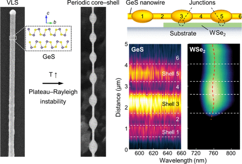
Figure 1
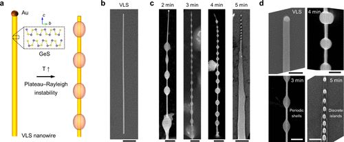
Figure 1. Periodic shell formation on a GeS van der Waals nanowire via the Plateau–Rayleigh (P-R) instability. (a) Schematic illustration showing the formation of a periodic core–shell GeS nanowire from a VLS-grown straight nanowire, driven by the P-R instability at elevated temperature. Inset highlights orthorhombic GeS crystal structure where the vdW layers are transversely stacked relative to the axial direction. (b) SEM image of a straight GeS nanowire grown from an Au catalyst. The growth was conducted by nucleating at 380 °C for 3 min and elongating at 300 °C for 10 min. The pressure and Ar carrier gas flow rate were 20 Torr and 50 sccm, respectively. Scale bar, 1 μm. (c) SEM images showing the evolution of periodic core–shell structure. The growth was continued at 390 °C, under a pressure of 20 Torr and an Ar gas flow rate of 50 sccm, for growth times (tg) of 2–5 min (from left to right). Scale bars, 500 nm. (d) Magnified SEM plan views of GeS nanowires. Top left: A straight VLS nanowire with its growth front decorated with an Au catalytic droplet. Bottom left and Top right: Core–shell structures showing periodic shells at tg = 3 and 4 min, respectively. Bottom right: Discrete islands formed by the P-R instability at tg = 5 min. Scale bars, 200 nm.
Figure 2
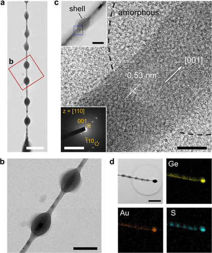
Figure 2. Structural analysis of GeS periodic shell nanowires. (a) Bright-field TEM image of a GeS periodic shell nanowire (tg = 3 min). Scale bar, 500 nm. (b) Magnified TEM image of the region marked by the red square in (a). Scale bar, 200 nm. (c) High-resolution TEM image of the crystalline core and amorphous shell, corresponding to the area in the blue box region of the top-left inset. The image shows a lattice spacing of 0.53 nm and confirms the axial orientation is along the [001] direction. Bottom left inset: Corresponding SAED pattern from a [110] zone axis, validating the axial orientation along the c-axis. Scale bars, 10 nm (main image), 100 nm (top-left inset), and 100 nm–1. (d) EDS elemental mapping images of the GeS periodic shell nanowire. Scale bar, 500 nm.
Figure 3
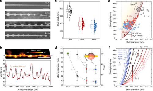
Figure 3. Time-dependent periodic shell formation on GeS nanowire sidewalls. (a) SEM images showing the morphological evolution of GeS nanowire. A VLS nanowire with straight and uniform sidewall grown at 300 °C, periodic core–shell structures after growth for 2, 3, and 4 min at 390 °C (top to bottom). Scale bars, 500 nm. (b) AFM height map (top) and corresponding axial line profile (bottom) of a representative periodic core–shell nanowire with tg = 3 min. The profile shows a periodic height modulation superimposed on a gradual decrease in the average height from base (left) to tip (right). Scale bar, 1 μm. (c) Statistical distribution of the shell pitch as a function of growth time. (d) Nanowire (core) diameter (Dc, left axis) and the shell-to-core diameter ratio (Ds/Dc, right axis) as a function of growth time. The inset illustrates the definitions of these parameters. (e) Experimentally measured correlation between shell pitch and shell diameter for different growth times. The data are overlaid with a theoretical model prediction, where the solid red line indicates the thermodynamic threshold for spontaneous periodic shell formation (ΔGs < 0) for Dc = 50 nm and Dw = 100 nm, where Dw is the fictitious diameter of a conformal shell. (f) Theoretical stability diagram derived from the model, showing the calculated instability threshold as a function of shell diameter and pitch for various core and fictitious conformal shell diameters.
Figure 4
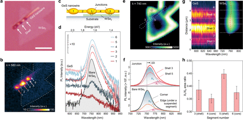
Figure 4. Spatially modulated optoelectronic properties of GeS/WSe2 mixed-dimensional vdW heterostructure. (a) OM image of a periodic core–shell GeS nanowire transferred onto a monolayer WSe2. Scale bar, 3 μm. (b) PL intensity map corresponding to the GeS emission (λ = 580 nm), showing emission is brightest at the shell segments (1, 3, 5). (c) Schematic illustration of the heterostructure, highlighting the direct vdW junctions formed between the GeS shells (i.e., 3, 5) and the underlying WSe2. (d) PL spectra from numbered nanowire points and a bare WSe2 region (black), showing broad GeS (λ ≤ 680 nm) and sharp WSe2 (∼750 nm) exciton peaks. Spectra are offset for clarity. (e) PL intensity map of the WSe2 emission (λ = 740 nm), confirming strong, localized PL quenching at the GeS shell junctions. Dashed circles indicate the locations of the spectra shown in (f). (f) Deconvoluted PL spectra from representative ‘Junction’ (top) and ‘Pristine’ (bottom) regions, as marked in (e). The peaks are fitted to a neutral exciton (X0) and a lower-energy trion (XT). The junction spectra exhibit a significant redshift (Δλ = 10 nm) and an enhanced trion contribution. (g) Spatially resolved hyperspectral maps along the nanowire axis, showing the direct correlation between the GeS PL intensity modulation and the redshift of the WSe2 PL at the shell junctions. Color scales are identical to those in (b) and (e). (h) Ratio of the integrated trion-to-exciton peak areas for junction segments located on the WSe2 flake, confirming a local enhancement of the trion population specifically at the shell junctions (3 and 5).
References
This article references 44 other publications.
- 1Eggers, J. Nonlinear dynamics and breakup of free-surface flows. Rev. Mod. Phys. 1997, 69 (3), 865, DOI: 10.1103/RevModPhys.69.865There is no corresponding record for this reference.
- 2Barker, B.; Bell, J. B.; Garcia, A. L. Fluctuating hydrodynamics and the Rayleigh-Plateau instability. Proc. Natl. Acad. Sci. U. S. A. 2023, 120 (30), e2306088120 DOI: 10.1073/pnas.2306088120There is no corresponding record for this reference.
- 3Rayleigh, L. On The Instability Of Jets. Proc. London Math. Soc. 1878, s1–10 (1), 4– 13, DOI: 10.1112/plms/s1-10.1.4There is no corresponding record for this reference.
- 4Eggers, J.; Villermaux, E. Physics of liquid jets. Rep. Prog. Phys. 2008, 71 (3), 036601 DOI: 10.1088/0034-4885/71/3/036601There is no corresponding record for this reference.
- 5Day, R. W.; Mankin, M. N.; Gao, R.; No, Y.-S.; Kim, S.-K.; Bell, D. C.; Park, H.-G.; Lieber, C. M. Plateau–Rayleigh crystal growth of periodic shells on one-dimensional substrates. Nat. Nanotechnol. 2015, 10 (4), 345– 352, DOI: 10.1038/nnano.2015.23There is no corresponding record for this reference.
- 6Day, R. W.; Mankin, M. N.; Lieber, C. M. Plateau–Rayleigh Crystal Growth of Nanowire Heterostructures: Strain-Modified Surface Chemistry and Morphological Control in One, Two, and Three Dimensions. Nano Lett. 2016, 16 (4), 2830– 2836, DOI: 10.1021/acs.nanolett.6b00629There is no corresponding record for this reference.
- 7Xue, Z.; Xu, M.; Zhao, Y.; Wang, J.; Jiang, X.; Yu, L.; Wang, J.; Xu, J.; Shi, Y.; Chen, K.; Roca i Cabarrocas, P. Engineering island-chain silicon nanowires via a droplet mediated Plateau–Rayleigh transformation. Nat. Commun. 2016, 7 (1), 12836, DOI: 10.1038/ncomms12836There is no corresponding record for this reference.
- 8Shao, Z.-C.; Jiang, X.; Zhang, C.; Wang, T.; Wang, Y.-R.; Liu, G.-Q.; Huang, Z.-Y.; Zhang, Y.-Z.; Wu, L.; Hou, Z.-H. Plateau–Rayleigh Instability in Soft-Lattice Inorganic Solids. J. Am. Chem. Soc. 2024, 146 (49), 33774– 33783, DOI: 10.1021/jacs.4c11866There is no corresponding record for this reference.
- 9Custer, J. P.; Low, J. D.; Hill, D. J.; Teitsworth, T. S.; Christesen, J. D.; McKinney, C. J.; McBride, J. R.; Brooke, M. A.; Warren, S. C.; Cahoon, J. F. Ratcheting quasi-ballistic electrons in silicon geometric diodes at room temperature. Science 2020, 368 (6487), 177– 180, DOI: 10.1126/science.aay8663There is no corresponding record for this reference.
- 10White, K. L.; Umantsev, M. A.; Low, J. D.; Custer, J. P.; Cahoon, J. F. Influence of Geometry on Quasi-Ballistic Behavior in Silicon Nanowire Geometric Diodes. ACS Appl. Nano Mater. 2023, 6 (7), 5117– 5126, DOI: 10.1021/acsanm.2c04666There is no corresponding record for this reference.
- 11White, K. L.; Rogelberg, G. V.; Custer, J. P.; Cahoon, J. F. Omega-Gate Silicon Nanowire Geometric Diodes with Reconfigurable Self-Switching Operation and THz Rectification. Adv. Electron. Mater. 2024, 10 (1), 2300466 DOI: 10.1002/aelm.202300466There is no corresponding record for this reference.
- 12Malhotra, A.; Tutuncuoglu, G.; Kommandur, S.; Creamer, P.; Rajan, A.; Mohabir, A.; Yee, S.; Filler, M. A.; Maldovan, M. Impact of Porosity and Boundary Scattering on Thermal Transport in Diameter-Modulated Nanowires. ACS Appl. Mater. Interfaces 2022, 14 (1), 1740– 1746, DOI: 10.1021/acsami.1c20242There is no corresponding record for this reference.
- 13Blandre, E.; Chaput, L.; Merabia, S.; Lacroix, D.; Termentzidis, K. Modeling the reduction of thermal conductivity in core/shell and diameter-modulated silicon nanowires. Phys. Rev. B 2015, 91 (11), 115404 DOI: 10.1103/PhysRevB.91.115404There is no corresponding record for this reference.
- 14Ko, M.; Baek, S. H.; Song, B.; Kang, J. W.; Kim, S. A.; Cho, C. H. Periodically Diameter-Modulated Semiconductor Nanowires for Enhanced Optical Absorption. Adv. Mater. 2016, 28 (13), 2504– 2510, DOI: 10.1002/adma.201505144There is no corresponding record for this reference.
- 15Oliveira, D. S.; Tizei, L. H. G.; Ugarte, D.; Cotta, M. A. Spontaneous Periodic Diameter Oscillations in InP Nanowires: The Role of Interface Instabilities. Nano Lett. 2013, 13 (1), 9– 13, DOI: 10.1021/nl302891bThere is no corresponding record for this reference.
- 16Sutter, P.; Sutter, E. Tunable 1D van der Waals Nanostructures by Vapor-Liquid-Solid Growth. Acc. Chem. Res. 2023, 56 (22), 3235– 3245, DOI: 10.1021/acs.accounts.3c00502There is no corresponding record for this reference.
- 17Sutter, E.; Kisslinger, K.; Wu, L.; Zhu, Y.; Yang, S.; Camino, F.; Nam, C. Y.; Sutter, P. Single Crystalline GeSe Van Der Waals Ribbons With Uniform Layer Stacking, High Carrier Mobility, and Adjustable Edge Morphology. Small 2024, 20 (50), 2406129 DOI: 10.1002/smll.202406129There is no corresponding record for this reference.
- 18Liu, Y.; Jin, L.; Pandey, T.; Sun, H.; Liu, Y.; Li, X.; Rodriguez, A.; Wang, Y.; Zhou, T.; Chen, R. Anomalous thermal transport in Eshelby twisted van der Waals nanowires. Nat. Mater. 2025, 24 (5), 728– 734, DOI: 10.1038/s41563-024-02108-3There is no corresponding record for this reference.
- 19Song, H.; Ji, S.; Kang, S. G.; Shin, N. Contact Geometry-Dependent Excitonic Emission in Mixed-Dimensional van der Waals Heterostructures. ACS Nano 2024, 18 (29), 19179– 19189, DOI: 10.1021/acsnano.4c04770There is no corresponding record for this reference.
- 20Jiang, K.; You, Q.; Zheng, Y.; Fang, F.; Xie, Z.; Li, H.; Wan, Y.; Han, C.; Shi, Y. Oriented Epitaxial Growth of Mixed-Dimensional van der Waals Heterostructures with One-Dimensional (1D) Bi2S3 Nanowires and Two-Dimensional (2D) WS2 Monolayers for Performance-Enhanced Photodetectors. Nano Lett. 2024, 24 (45), 14437– 14444, DOI: 10.1021/acs.nanolett.4c04455There is no corresponding record for this reference.
- 21Lv, Q.; Tan, J.; Wang, Z.; Gu, P.; Liu, H.; Yu, L.; Wei, Y.; Gan, L.; Liu, B.; Li, J.; Kang, F.; Cheng, H.-M.; Xiong, Q.; Lv, R. Ultrafast charge transfer in mixed-dimensional WO3-x nanowire/WSe2 heterostructures for attomolar-level molecular sensing. Nat. Commun. 2023, 14 (1), 2717, DOI: 10.1038/s41467-023-38198-xThere is no corresponding record for this reference.
- 22Yang, X.; Wu, R.; Zheng, B.; Luo, Z.; You, W.; Liu, H.; Li, L.; Zhang, Y.; Tan, Q.; Liang, D. A Waveguide-Integrated Two-Dimensional Light-Emitting Diode Based on p-Type WSe2/n-Type CdS Nanoribbon Heterojunction. ACS Nano 2022, 16 (3), 4371– 4378, DOI: 10.1021/acsnano.1c10607There is no corresponding record for this reference.
- 23Sutter, E.; Sutter, P. 1D Wires of 2D Layered Materials: Germanium Sulfide Nanowires as Efficient Light Emitters. ACS Appl. Nano Mater. 2018, 1 (3), 1042– 1049, DOI: 10.1021/acsanm.7b00053There is no corresponding record for this reference.
- 24Sutter, P.; Idrobo, J. C.; Sutter, E. Van der Waals Nanowires with Continuously Variable Interlayer Twist and Twist Homojunctions. Adv. Funct. Mater. 2021, 31 (9), 2006412 DOI: 10.1002/adfm.202006412There is no corresponding record for this reference.
- 25Sutter, E.; French, J. S.; Sutter, P. Tunable Layer Orientation and Morphology in Vapor–Liquid–Solid Growth of One-Dimensional GeS van der Waals Nanostructures. Chem. Mater. 2021, 33 (11), 3980– 3988, DOI: 10.1021/acs.chemmater.1c00289There is no corresponding record for this reference.
- 26Dolado, J.; Renforth, K. L.; Nunn, J. E.; Hindsmarsh, S. A.; Hidalgo, P.; Sánchez, A. M.; Méndez, B. Zn2GeO4/SnO2 Nanowire Heterostructures Driven by Plateau–Rayleigh Instability. Cryst. Growth Des. 2020, 20 (1), 506– 513, DOI: 10.1021/acs.cgd.9b01494There is no corresponding record for this reference.
- 27Mead-Hunter, R.; King, A. J.; Mullins, B. J. Plateau Rayleigh instability simulation. Langmuir 2012, 28 (17), 6731– 6735, DOI: 10.1021/la300622hThere is no corresponding record for this reference.
- 28Shabahang, S.; Kaufman, J. J.; Deng, D. S.; Abouraddy, A. F. Observation of the Plateau–Rayleigh capillary instability in multi-material optical fibers. Appl. Phys. Lett. 2011, 99 (16), 161909 DOI: 10.1063/1.3653247There is no corresponding record for this reference.
- 29Malone, B. D.; Kaxiras, E. Quasiparticle band structures and interface physics of SnS and GeS. Phys. Rev. B 2013, 87 (24), 245312 DOI: 10.1103/PhysRevB.87.245312There is no corresponding record for this reference.
- 30Li, C.; Yu, Y.; Chi, M.; Cao, L. Epitaxial Nanosheet-Nanowire Heterostructures. Nano Lett. 2013, 13 (3), 948– 953, DOI: 10.1021/nl303876aThere is no corresponding record for this reference.
- 31Ribeiro, H. B.; Ramos, S. L. L. M.; Seixas, L.; de Matos, C. J. S.; Pimenta, M. A. Edge phonons in layered orthorhombic GeS and GeSe monochalcogenides. Phys. Rev. B 2019, 100 (9), 094301 DOI: 10.1103/PhysRevB.100.094301There is no corresponding record for this reference.
- 32Hsueh, H. C.; Warren, M. C.; Vass, H.; Ackland, G. J.; Clark, S. J.; Crain, J. Vibrational properties of the layered semiconductor germanium sulfide under hydrostatic pressure: Theory and experiment. Phys. Rev. B 1996, 53 (22), 14806, DOI: 10.1103/PhysRevB.53.14806There is no corresponding record for this reference.
- 33Jadczak, J.; Andrzejewski, J.; Debus, J.; Ho, C. H.; Bryja, L. Resonant Exciton Scattering Reveals Raman Forbidden Phonon Modes in Layered GeS. J. Phys. Chem. Lett. 2023, 14 (17), 3986– 3994, DOI: 10.1021/acs.jpclett.3c00783There is no corresponding record for this reference.
- 34Dayeh, S. A.; Yu, E. T.; Wang, D. Surface Diffusion and Substrate-Nanowire Adatom Exchange in InAs Nanowire Growth. Nano Lett. 2009, 9 (5), 1967– 1972, DOI: 10.1021/nl900191wThere is no corresponding record for this reference.
- 35Dayeh, S. A.; Mack, N. H.; Huang, J. Y.; Picraux, S. T. Advanced core/multishell germanium/silicon nanowire heterostructures: The Au-diffusion bottleneck. Appl. Phys. Lett. 2011, 99 (2), 023102 DOI: 10.1063/1.3567932There is no corresponding record for this reference.
- 36Lee, Y.; Shin, N. Mechanistic insights into diffusion-controlled 2D WSe2 growth via chemical vapor deposition in confined spaces. FlatChem. 2025, 51, 100863 DOI: 10.1016/j.flatc.2025.100863There is no corresponding record for this reference.
- 37Suzuki, H.; Hashimoto, R.; Misawa, M.; Liu, Y.; Kishibuchi, M.; Ishimura, K.; Tsuruta, K.; Miyata, Y.; Hayashi, Y. Surface Diffusion-Limited Growth of Large and High-Quality Monolayer Transition Metal Dichalcogenides in Confined Space of Microreactor. ACS Nano 2022, 16 (7), 11360– 11373, DOI: 10.1021/acsnano.2c05076There is no corresponding record for this reference.
- 38Li, S.; Hong, J.; Gao, B.; Lin, Y.-C.; Lim, H. E.; Lu, X.; Wu, J.; Liu, S.; Tateyama, Y.; Sakuma, Y.; Tsukagoshi, K.; Suenaga, K.; Taniguchi, T. Tunable Doping of Rhenium and Vanadium into Transition Metal Dichalcogenides for Two-Dimensional Electronics. Adv. Sci. 2021, 8 (11), 2004438 DOI: 10.1002/advs.202004438There is no corresponding record for this reference.
- 39Kim, J.; Jin, C.; Chen, B.; Cai, H.; Zhao, T.; Lee, P.; Kahn, S.; Watanabe, K.; Taniguchi, T.; Tongay, S.; Crommie, M. F.; Wang, F. Observation of ultralong valley lifetime in WSe2/MoS2 heterostructures. Sci. Adv. 2017, 3 (7), 1700518 DOI: 10.1126/sciadv.1700518There is no corresponding record for this reference.
- 40Musin, I. R.; Boyuk, D. S.; Filler, M. A. Surface chemistry controlled diameter-modulated semiconductor nanowire superstructures. J. Vac. Sci. Technol. B 2013, 31 (2), 020603 DOI: 10.1116/1.4792660There is no corresponding record for this reference.
- 41Christesen, J. D.; Pinion, C. W.; Hill, D. J.; Kim, S.; Cahoon, J. F. Chemically Engraving Semiconductor Nanowires: Using Three-Dimensional Nanoscale Morphology to Encode Functionality from the Bottom Up. J. Phys. Chem. Lett. 2016, 7 (4), 685– 692, DOI: 10.1021/acs.jpclett.5b02444There is no corresponding record for this reference.
- 42Sharmila, B.; Dwivedi, P. MoS2/SiNWs heterostructure based repeatable and highly responsive photodetector. Opt. Mater. 2022, 133, 112918 DOI: 10.1016/j.optmat.2022.112918There is no corresponding record for this reference.
- 43Ananth, R.; Utama, M. I. B.; Xu, D. D.; Vong, A. F.; Sadhukhan, T.; Zeng, H.; López-Arteaga, R.; Wang, W.; Namgung, S. D.; Gavin, S. C. Enhanced spectral purity of WSe2 quantum emitters via conformal organic adlayers. Sci. Adv. 2025, 11 (40), eady7557 DOI: 10.1126/sciadv.ady7557There is no corresponding record for this reference.
- 44Wu, C.-H.; Reep, T.; Huang, Y.; Brems, S.; Haffner, C.; Huyghebaert, C.; Kuyken, B.; Van Campenhout, J.; Pantouvaki, M.; Van Thourhout, D. Low-loss phase modulation using a MoS2 monolayer integrated on silicon waveguides. 2D Mater. 2025, 12 (4), 045006 DOI: 10.1088/2053-1583/ade9d9There is no corresponding record for this reference.
Supporting Information
Supporting Information
The Supporting Information is available free of charge at https://pubs.acs.org/doi/10.1021/acs.nanolett.5c04385.
SEM image of Au nanoparticles dispersed on Si substrate and optical microscopic images of as-grown and dry-transferred GeS nanowires. TEM and EDS analyses of straight and core–shell nanowires. EDS spectra of core–shell GeS nanowires. Raman spectrum of a periodic core–shell GeS nanowire. Additional SEM images of periodic core–shell GeS nanowires at different growth durations. Statistical distributions of shell diameters and shell contact angles as a function of growth time. Comparison of shell-thicknesses measurements by AFM and SEM. Shell and core diameter comparison between upper and lower segments. Comparison of core and shell diameters at the upper and lower segments in periodic nanowires. Schematic comparing periodic shell and conformal shell structures. PL measurements on a core–shell GeS nanowire. PL spectra comparison between shell contact and intershell regions. UPS analysis of GeS. Superimposed PL intensity maps at the GeS and WSe2 emission wavelengths. PL peak deconvolution near the GeS/WSe2 junction regions. Comparison of P-R instability in nanowires reported in previous studies. (PDF)
Terms & Conditions
Most electronic Supporting Information files are available without a subscription to ACS Web Editions. Such files may be downloaded by article for research use (if there is a public use license linked to the relevant article, that license may permit other uses). Permission may be obtained from ACS for other uses through requests via the RightsLink permission system: http://pubs.acs.org/page/copyright/permissions.html.